
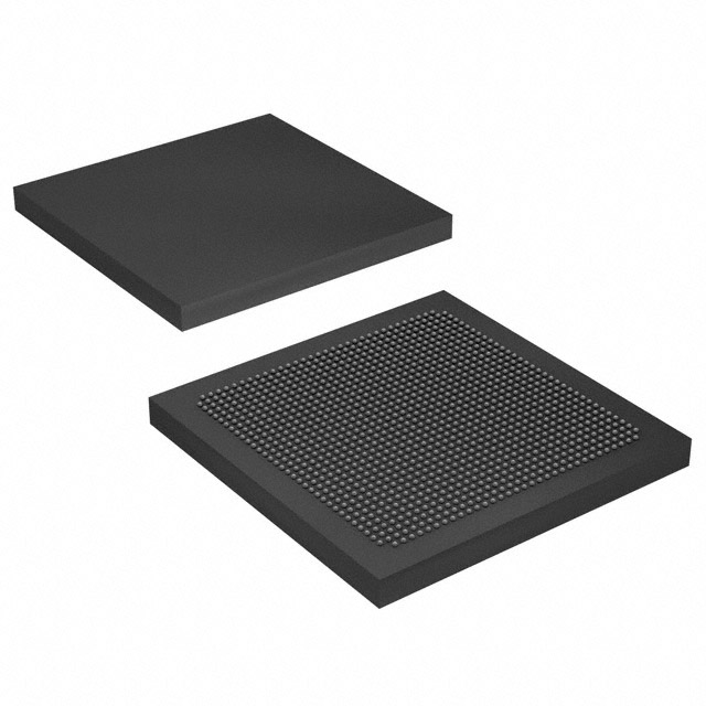
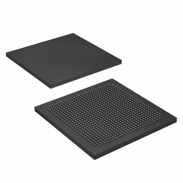
10AX027H1F34E1HG
| Part Description |
Arria 10 GX Field Programmable Gate Array (FPGA) IC 384 17870848 270000 1152-BBGA, FCBGA |
|---|---|
| Quantity | 1,374 Available (as of June 15, 2026) |

| Product Category | Field Programmable Gate Array (FPGA) |
|---|---|
| Manufacturer | Intel |
| Manufacturing Status | Active |
| Manufacturer Standard Lead Time | 16 Weeks |
| Datasheet |
Specifications & Environmental
| Device Package | 1152-FCBGA (35x35) | Grade | Extended | Operating Temperature | 0°C – 100°C | ||
|---|---|---|---|---|---|---|---|
| Package / Case | 1152-BBGA, FCBGA | Number of I/O | 384 | Voltage | 870 mV - 980 mV | ||
| Mounting Method | Surface Mount | RoHS Compliance | RoHS Compliant | REACH Compliance | REACH Unaffected | ||
| Moisture Sensitivity Level | 3 (168 Hours) | Number of LABs/CLBs | 101620 | Number of Logic Elements/Cells | 270000 | ||
| Number of Gates | N/A | ECCN | 5A002A1 | HTS Code | 8542.39.0001 | ||
| Qualification | N/A | Total RAM Bits | 17870848 |
Overview of 10AX027H1F34E1HG – Arria 10 GX FPGA, 270,000 logic elements, 17,870,848 RAM bits, 384 I/Os, 1152‑FCBGA
The 10AX027H1F34E1HG is an Intel Arria 10 GX field-programmable gate array (FPGA) offered in a 1152‑FCBGA (35×35) surface-mount package. It delivers the mid‑range, high‑performance and power‑efficient architecture of the Arria 10 family optimized for complex, power‑sensitive designs.
This device targets applications across wireless, wireline, broadcast, computing and storage, medical and defense markets where large logic capacity, embedded RAM and flexible I/O are required. The device combines substantial on‑chip memory and DSP capability with family-level features such as high-speed serial transceivers and PCIe/ethernet hard IP (as described for the Arria 10 family).
Key Features
- Logic Capacity — 270,000 logic elements to implement complex mid‑range FPGA designs and algorithm acceleration.
- On‑chip Memory — 17,870,848 total RAM bits for large embedded data storage and buffering without immediate dependence on external memory.
- I/O and Interfaces — 384 general‑purpose I/Os and support for standard external memory interfaces; family documentation describes PCIe and high‑speed Ethernet/Interlaken hard IP options.
- DSP and Processing Blocks — Arria 10 family features include variable‑precision DSP blocks for signal processing and algorithm implementation.
- Clocking and PLLs — Advanced clock networks and PLL clock sources are available as part of the Arria 10 device architecture for flexible timing and synchronization.
- Package & Mounting — 1152‑FCBGA (35×35) package, surface‑mount for high‑density board integration.
- Power Supply — Device core supply range of 870 mV to 980 mV and family‑level power‑saving technologies aimed at improving energy efficiency.
- Operating Range & Grade — Extended grade with specified operating temperature range of 0 °C to 100 °C; RoHS compliant.
Typical Applications
- Wireless infrastructure — Channel and switch cards in remote radio heads and mobile backhaul systems that require significant logic and on‑chip RAM.
- Wireline and optical transport — 40G/100G muxponders, transponders and line cards leveraging high logic density and SerDes/PCS family features.
- Broadcast and Pro AV — Studio switches, video processing and professional audio/video equipment using embedded memory and DSP resources.
- Compute and Storage Acceleration — Server acceleration, flash cache and cloud compute functions that benefit from on‑chip memory and large logic arrays.
- Medical and Defense Systems — Diagnostic imaging, radar and secure communications implementations that use the device’s processing and I/O capabilities within the stated temperature range.
Unique Advantages
- High logic density: 270,000 logic elements provide the capacity needed for sophisticated mid‑range FPGA designs and hardware acceleration.
- Significant on‑chip memory: 17,870,848 RAM bits enable larger buffers and local data storage to reduce external memory dependency and simplify board design.
- Rich I/O resources: 384 I/Os plus support for standard memory interfaces and family‑level high‑speed I/O blocks ease system integration and connectivity.
- Power‑aware operation: Documented Arria 10 family power‑saving technologies combined with a defined core supply range (870–980 mV) support energy‑sensitive designs.
- Board‑level integration: 1152‑FCBGA surface‑mount package in a 35×35 footprint enables high‑density placement on modern PCBs.
- Extended operating grade: Specified 0 °C to 100 °C operating temperature and RoHS compliance for standard commercial and extended applications.
Why Choose 10AX027H1F34E1HG?
The 10AX027H1F34E1HG brings the Arria 10 GX family’s mid‑range performance and power efficiency into a compact, high‑capacity FPGA package. With 270,000 logic elements, almost 18 Mb of on‑chip RAM and 384 I/Os, it is positioned for designs that require substantial logic, embedded memory and flexible I/O without moving to larger device classes.
This part is appropriate for engineers designing wireless, wireline, broadcast, compute/storage, medical and defense applications that rely on the Arria 10 device architecture and documented family features. It offers a balance of integration, power management and board‑level packaging for scalable deployments backed by Arria 10 device documentation.
Request a quote or submit an inquiry to get pricing and availability for the 10AX027H1F34E1HG. Our team will respond with ordering and support information promptly.


Date Founded: 1968
Headquarters: Santa Clara, California, USA
Employees: 130,000+
Revenue: $54.23 Billion
Certifications and Memberships: ISO9001:2015, ISO14001:2015, ISO17025:2017, ISO27001:2022, ISO45001:2018, ISO50001:2018


