
10AX027H2F34E2SG
| Part Description |
Arria 10 GX Field Programmable Gate Array (FPGA) IC 384 17870848 270000 1152-BBGA, FCBGA |
|---|---|
| Quantity | 825 Available (as of June 10, 2026) |

| Product Category | Field Programmable Gate Array (FPGA) |
|---|---|
| Manufacturer | Intel |
| Manufacturing Status | Active |
| Manufacturer Standard Lead Time | 16 Weeks |
| Datasheet |
Specifications & Environmental
| Device Package | 1152-FBGA, FC (35x35) | Grade | Extended | Operating Temperature | 0°C – 100°C | ||
|---|---|---|---|---|---|---|---|
| Package / Case | 1152-BBGA, FCBGA | Number of I/O | 384 | Voltage | 870 mV - 980 mV | ||
| Mounting Method | Surface Mount | RoHS Compliance | RoHS Compliant | REACH Compliance | REACH Unaffected | ||
| Moisture Sensitivity Level | 3 (168 Hours) | Number of LABs/CLBs | 101620 | Number of Logic Elements/Cells | 270000 | ||
| Number of Gates | N/A | ECCN | 5A002A1 | HTS Code | 8542.39.0001 | ||
| Qualification | N/A | Total RAM Bits | 17870848 |
Overview of 10AX027H2F34E2SG – Arria 10 GX Field Programmable Gate Array (FPGA) 1152-BBGA
The 10AX027H2F34E2SG is an Arria 10 GX series FPGA in a 1152-BBGA (FCBGA) package designed for mid-range, performance-sensitive applications. As part of the Intel Arria 10 device family, it combines high logic capacity, significant embedded memory, programmable DSP and transceiver resources, and flexible clocking to address data-path and interface-intensive designs.
This device targets markets such as wireless infrastructure, wireline communications, broadcast, computing and storage, and specialized imaging and defense systems where configurable logic, I/O density, and integrated building blocks accelerate system design and differentiation.
Key Features
- Logic Capacity Provides 270,000 logic elements for implementing complex custom logic and control functions.
- Embedded Memory Total of 17,870,848 RAM bits to support large on-chip buffers, caches, and packet or frame storage.
- I/O Density 384 I/O pins to support wide external interfaces and multiple memory or protocol connections.
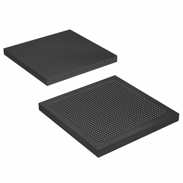
- Package & Mounting 1152-BBGA (1152-FBGA, FC, 35×35) surface-mount package for high-pin-count board designs.
- Voltage & Power Operates from a core voltage supply range of 870 mV to 980 mV.
- Operating Range & Grade Specified operating temperature 0°C to 100°C and delivered in Extended grade.
- Programmable DSP and Memory Blocks Arria 10 devices include variable-precision DSP blocks and multiple embedded memory block types for signal processing and buffering.
- Clocking and PLLs Comprehensive clock networks with PLL clock sources and fractional synthesis options to support diverse timing domains.
- High-Speed I/O and Protocol IP Arria 10 device family provides low-power serial transceivers and hard IP options such as PCIe Gen1/Gen2/Gen3 and enhanced PCS IP for Interlaken and 10 Gbps Ethernet.
Typical Applications
- Wireless Infrastructure Used in channel and switch cards for remote radio heads and mobile backhaul to implement radio and transport logic with embedded DSP and I/O resources.
- Wireline Communications Applicable to 40G/100G muxponders, transponders, and line cards where high-speed serial transceivers and protocol hard IP accelerate interface implementation.
- Broadcast and Media Suitable for studio switches, professional audio/video processing, and videoconferencing equipment that require large on-chip memory and flexible logic for real-time workflows.
- Computing and Storage Fits roles in server acceleration, flash cache, and cloud compute systems where programmable acceleration and on-chip buffering reduce system latency.
Unique Advantages
- High Logic Density: 270,000 logic elements enable complex control, protocol handling, and custom datapath implementations on a single device.
- Large On-chip Memory: Nearly 18 Mbits of RAM bits support deep buffering, packet storage, and memory-intensive algorithms without immediate dependence on external DRAM.
- Rich I/O and Interface Support: 384 I/Os combined with Arria 10 serial/transceiver and hard IP capabilities simplify multi-protocol board designs and high-bandwidth connectivity.
- Configurable Signal Processing: Variable-precision DSP blocks and embedded memory blocks enable implementation of tailored signal processing pipelines and accelerators.
- Flexible Clocking: Advanced clock networks and PLL clock sources, including fractional synthesis, help align multiple timing domains and support precise interface timing.
- Board-level Integration: 1152-BBGA surface-mount package (35×35) provides high pin-count in a compact footprint for dense PCB designs.
Why Choose 10AX027H2F34E2SG?
The 10AX027H2F34E2SG Arria 10 GX FPGA combines substantial logic capacity, large embedded memory, and extensive I/O in a high-pin-count FCBGA package, making it well-suited for mid-range systems that require configurable datapath acceleration and broad interface support. Its feature set—programmable DSP blocks, advanced clocking, and integrated protocol hard IP—supports rapid development of communications, media, and compute applications.
Designed for engineers seeking a balance of performance, integration, and power efficiency within the Arria 10 family, this device provides a scalable platform for designs that need embedded memory, multiple I/Os, and flexible transceiver/clock resources while operating over a 0°C to 100°C range and an 870–980 mV core supply window.
Request a quote or submit a sales inquiry to evaluate the 10AX027H2F34E2SG for your next design project.


Date Founded: 1968
Headquarters: Santa Clara, California, USA
Employees: 130,000+
Revenue: $54.23 Billion
Certifications and Memberships: ISO9001:2015, ISO14001:2015, ISO17025:2017, ISO27001:2022, ISO45001:2018, ISO50001:2018


