
10AX027H2F34E1HG
| Part Description |
Arria 10 GX Field Programmable Gate Array (FPGA) IC 384 17870848 270000 1152-BBGA, FCBGA |
|---|---|
| Quantity | 307 Available (as of June 15, 2026) |

| Product Category | Field Programmable Gate Array (FPGA) |
|---|---|
| Manufacturer | Intel |
| Manufacturing Status | Active |
| Manufacturer Standard Lead Time | 16 Weeks |
| Datasheet |
Specifications & Environmental
| Device Package | 1152-FCBGA (35x35) | Grade | Extended | Operating Temperature | 0°C – 100°C | ||
|---|---|---|---|---|---|---|---|
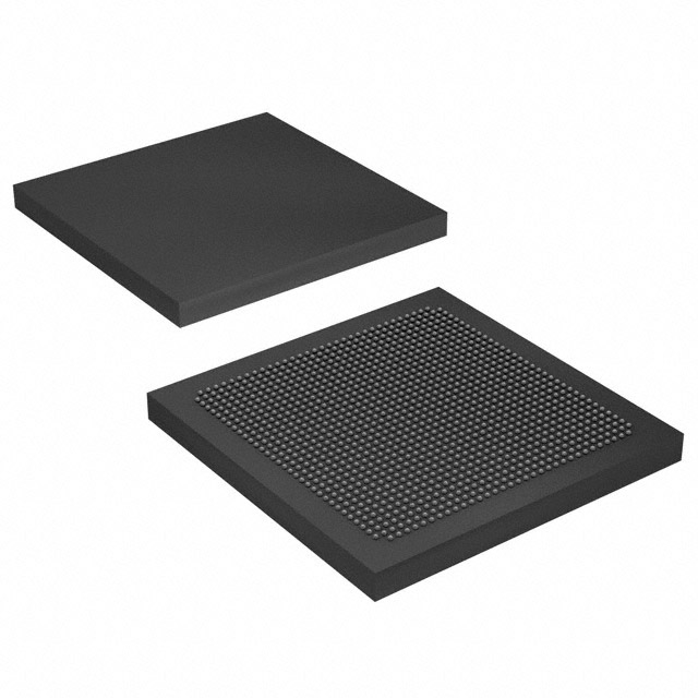
| Package / Case | 1152-BBGA, FCBGA | Number of I/O | 384 | Voltage | 870 mV - 980 mV | ||
| Mounting Method | Surface Mount | RoHS Compliance | RoHS Compliant | REACH Compliance | REACH Unaffected | ||
| Moisture Sensitivity Level | 3 (168 Hours) | Number of LABs/CLBs | 101620 | Number of Logic Elements/Cells | 270000 | ||
| Number of Gates | N/A | ECCN | 5A002A1 | HTS Code | 8542.39.0001 | ||
| Qualification | N/A | Total RAM Bits | 17870848 |
Overview of 10AX027H2F34E1HG – Arria 10 GX FPGA, 1152-FCBGA
The 10AX027H2F34E1HG is an Intel Arria 10 GX field programmable gate array (FPGA) in a 1152-ball FCBGA package. It is a 20 nm mid-range FPGA device intended for high-performance, power-sensitive applications across markets such as wireless, wireline, broadcast, computing and storage, medical, and military.
With large logic capacity, abundant embedded memory, and a broad I/O complement, this device targets midrange systems that require performance and integration while supporting platform-level features described in the Arria 10 device family overview.
Key Features
- Core Architecture Arria 10 GX family device built on a 20 nm process with adaptive logic modules and variable-precision DSP blocks as described in the device overview.
- Logic Capacity 270,000 logic elements to implement complex digital logic and signal-processing functions.
- Embedded Memory 17,870,848 total RAM bits for on-chip buffering, caches, and deep FIFOs.
- I/O and Connectivity 384 I/O pins to support broad external-device interfacing; the family overview also documents support for external memory interfaces and high-speed serial transceivers.
- Package & Mounting Supplied in a 1152-ball FCBGA (1152-BBGA) surface-mount package, supplier package dimension 35 × 35 mm.
- Power Supported core voltage range of 870 mV to 980 mV and family-level power-saving technologies described in the device overview.
- Reliability & Configuration Family features listed include dynamic and partial reconfiguration options and SEU error detection and correction mechanisms.
- Operating Range Extended grade with an operating temperature range of 0 °C to 100 °C.
Typical Applications
- Wireless infrastructure Channel and switch cards in remote radio heads and mobile backhaul implementations that need programmable logic and DSP capability.
- Wireline networking 40G/100G muxponders, transponders, and line-card functions where high I/O count and on-chip memory support packet buffering and protocol processing.
- Broadcast and professional AV Studio switches, videoconferencing, and transport systems that require flexible I/O routing and real-time processing.
- Computing and storage acceleration Server acceleration, flash cache, and cloud computing use cases leveraging on-chip logic and memory.
- Medical and defense Diagnostic imaging, radar, and guidance systems that can use the device’s logic density and reconfiguration capabilities.
Unique Advantages
- High logic density: 270,000 logic elements enable implementation of complex algorithms and large-scale digital blocks on a single device.
- Substantial on-chip memory: 17,870,848 total RAM bits reduce reliance on external memory for many buffering and caching needs.
- Broad I/O support: 384 I/O pins provide flexibility for heterogeneous interfaces and multi-channel designs.
- System-level features: Family-level support for dynamic and partial reconfiguration and SEU detection/correction helps maintain uptime and enables field updates.
- Compact, surface-mount package: 1152-ball FCBGA (35 × 35 mm) balances high pin count with a compact footprint for board-level integration.
- Extended operating range: Extended-grade device rated from 0 °C to 100 °C for a wide set of commercial and industrial-adjacent applications.
Why Choose 10AX027H2F34E1HG?
The 10AX027H2F34E1HG delivers Arria 10 GX family capabilities—high logic capacity, significant embedded memory, and extensive I/O—in a compact 1152-ball FCBGA package. It is suited for midrange systems that require a balance of performance, on-chip integration, and reconfigurability.
Designers targeting wireless, networking, broadcast, compute acceleration, medical, or defense applications will find the device’s combination of logic elements, RAM bits, and family-level features useful for consolidating functions, simplifying board-level design, and enabling in-field flexibility.
Request a quote or submit an inquiry to discuss availability, pricing, and lead time for the 10AX027H2F34E1HG.


Date Founded: 1968
Headquarters: Santa Clara, California, USA
Employees: 130,000+
Revenue: $54.23 Billion
Certifications and Memberships: ISO9001:2015, ISO14001:2015, ISO17025:2017, ISO27001:2022, ISO45001:2018, ISO50001:2018


