
10AX032H2F34E1SG
| Part Description |
Arria 10 GX Field Programmable Gate Array (FPGA) IC 384 21040128 320000 1152-BBGA, FCBGA |
|---|---|
| Quantity | 258 Available (as of June 10, 2026) |

| Product Category | Field Programmable Gate Array (FPGA) |
|---|---|
| Manufacturer | Intel |
| Manufacturing Status | Discontinued |
| Manufacturer Standard Lead Time | 13 Weeks |
| Datasheet |
Specifications & Environmental
| Device Package | 1152-FCBGA (35x35) | Grade | Extended | Operating Temperature | 0°C – 100°C | ||
|---|---|---|---|---|---|---|---|
| Package / Case | 1152-BBGA, FCBGA | Number of I/O | 384 | Voltage | 870 mV - 980 mV | ||
| Mounting Method | Surface Mount | RoHS Compliance | RoHS Compliant | REACH Compliance | REACH Unaffected | ||
| Moisture Sensitivity Level | 3 (168 Hours) | Number of LABs/CLBs | 119900 | Number of Logic Elements/Cells | 320000 | ||
| Number of Gates | N/A | ECCN | 5A002A1 | HTS Code | 8542.39.0001 | ||
| Qualification | N/A | Total RAM Bits | 21040128 |
Overview of 10AX032H2F34E1SG – Arria 10 GX FPGA, 320,000 logic elements, 1152‑FCBGA
The 10AX032H2F34E1SG is an Intel Arria 10 GX family Field Programmable Gate Array (FPGA) in a 1152‑FCBGA package. It is a 20‑nm, mid‑range FPGA device engineered for high‑performance, power‑sensitive applications across communications, compute, broadcast and imaging markets.
With 320,000 logic elements, 21,040,128 bits of embedded RAM and 384 I/O, this device targets system designs requiring high logic density, substantial on‑chip memory and flexible I/O integration while operating within a supply range of 870 mV to 980 mV and an extended temperature grade of 0°C to 100°C.
Key Features
- Core Logic Density — 320,000 logic elements provide substantial programmable resources for complex digital designs and algorithm implementation.
- Adaptive Logic Resources — 119,900 adaptive logic modules for building wide combinational and sequential logic structures.
- On‑chip Memory — 21,040,128 total RAM bits to support buffering, caches and memory‑intensive functions without immediate external memory dependence.
- I/O and Interface Capability — 384 general‑purpose I/O pins to support multiple parallel buses, control interfaces and external memory connections.
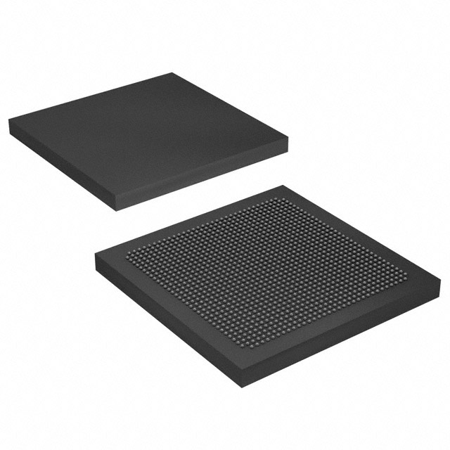
- Package and Mounting — 1152‑ball FCBGA surface‑mount package (1152‑FCBGA, 35×35) for high‑pin‑count, compact board integration.
- Power Supply — Core supply range of 870 mV to 980 mV enabling designs tuned for the device’s specified operating window.
- Operating Range and Grade — Extended grade with an operating temperature range of 0°C to 100°C suitable for many commercial and industrial‑adjacent applications.
- Series Capabilities (family‑level) — Arria 10 devices include power‑efficient architecture, embedded memory types and support for common high‑speed protocols and transceiver features as described in the device overview.
- Compliance — RoHS‑compliant for regulatory alignment in lead‑free assemblies.
Typical Applications
- Wireless Infrastructure — Implement channel processing, baseband functions and radio head logic leveraging high logic density and embedded RAM for buffering and DSP tasks.
- High‑Speed Networking — Use in line cards, muxponders and aggregation platforms where large I/O counts and on‑chip memory support packet processing and protocol handling.
- Broadcast and Professional Video — Realize switching, transcoding and transport functions that benefit from substantial programmable logic and memory resources.
- Compute and Storage Acceleration — Offload caching, data path acceleration and server acceleration tasks using abundant logic elements and embedded RAM.
- Medical and Imaging Systems — Support diagnostic imaging pipelines that require configurable logic, memory buffering and precise I/O control.
Unique Advantages
- High Logic Capacity: 320,000 logic elements enable implementation of large, complex designs on a single device, reducing board count and interconnect complexity.
- Substantial Embedded RAM: Over 21 million bits of on‑chip RAM provide local storage for packet buffers, frame buffers and intermediate data, minimizing external memory traffic.
- Extensive I/O Resources: 384 I/O pins allow broad peripheral connectivity and high‑pin‑count system integration without extensive external multiplexing.
- Compact, High‑Pin Package: The 1152‑FCBGA (35×35) package delivers high interconnect density in a surface‑mount form factor for space‑constrained systems.
- Family‑level Power Efficiency: Part of the Arria 10 family, which emphasizes performance with power‑saving technologies for energy‑sensitive designs.
- Documentation and Ecosystem: Supported by Arria 10 device documentation and device‑level resources for design guidance and integration best practices.
Why Choose 10AX032H2F34E1SG?
The 10AX032H2F34E1SG positions itself where high programmable capacity, significant on‑chip memory and broad I/O converge in a single 1152‑FCBGA package. It suits designs that require mid‑range FPGA performance with a focus on power efficiency and integration within the Arria 10 family framework.
Engineers building complex signal processing, networking, broadcast, compute acceleration or imaging systems will find the combination of logic density, embedded RAM and I/O count useful for consolidating functions, reducing board complexity and accelerating time to market, backed by the Arria 10 device resources and documentation.
Request a quote or submit an inquiry today to receive pricing, availability and support information for the 10AX032H2F34E1SG Arria 10 GX FPGA.


Date Founded: 1968
Headquarters: Santa Clara, California, USA
Employees: 130,000+
Revenue: $54.23 Billion
Certifications and Memberships: ISO9001:2015, ISO14001:2015, ISO17025:2017, ISO27001:2022, ISO45001:2018, ISO50001:2018


