
10AX057H3F34E2SG
| Part Description |
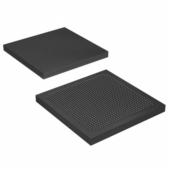
Arria 10 GX Field Programmable Gate Array (FPGA) IC 492 42082304 570000 1152-BBGA, FCBGA |
|---|---|
| Quantity | 849 Available (as of June 14, 2026) |

| Product Category | Field Programmable Gate Array (FPGA) |
|---|---|
| Manufacturer | Intel |
| Manufacturing Status | Active |
| Manufacturer Standard Lead Time | 12 Weeks |
| Datasheet |
Specifications & Environmental
| Device Package | 1152-FCBGA (35x35) | Grade | Extended | Operating Temperature | 0°C – 100°C | ||
|---|---|---|---|---|---|---|---|
| Package / Case | 1152-BBGA, FCBGA | Number of I/O | 492 | Voltage | 870 mV - 930 mV | ||
| Mounting Method | Surface Mount | RoHS Compliance | RoHS Compliant | REACH Compliance | REACH Unaffected | ||
| Moisture Sensitivity Level | 3 (168 Hours) | Number of LABs/CLBs | 217080 | Number of Logic Elements/Cells | 570000 | ||
| Number of Gates | N/A | ECCN | 3A001A7B | HTS Code | 8542.39.0001 | ||
| Qualification | N/A | Total RAM Bits | 42082304 |
Overview of 10AX057H3F34E2SG – Arria 10 GX Field Programmable Gate Array (FPGA), 1152‑FCBGA (35×35)
The 10AX057H3F34E2SG is an Intel Arria 10 GX FPGA device in a 1152‑ball FCBGA (35×35 mm) package. It delivers a mid-range, 20 nm FPGA architecture designed for high-performance, power-efficient implementations across communications, broadcast, compute and imaging applications.
Built for designs that require large programmable logic and embedded memory alongside advanced I/O and transceiver features, this device combines significant logic and RAM capacity with support for high‑speed serial interfaces and flexible clocking and reconfiguration capabilities.
Key Features
- Logic Capacity — 570,000 logic elements provide extensive programmable fabric for complex digital logic, signal processing, and control functions.
- Embedded Memory — 42,082,304 total RAM bits for on‑chip data buffering, frame storage, and intermediate processing.
- I/O Density — 492 I/O pins to support broad peripheral connectivity and multi‑channel interfacing requirements.
- Package — 1152‑FCBGA (35×35) supplier package for high‑pin‑count board designs and dense routing.
- Power and Voltage — Core supply operating range of 0.870 V to 0.930 V for the device core.
- Temperature & Grade — Extended grade operation from 0 °C to 100 °C suitable for demanding commercial and telecom environments.
- High‑Speed Interfaces (Series Features) — Series documentation highlights integrated low‑power serial transceivers, PCIe Gen1/Gen2/Gen3 Hard IP, and support for 10 Gbps Ethernet and Interlaken protocols for scalable link implementations.
- DSP and Clocking (Series Features) — Variable‑precision DSP blocks and comprehensive clock networks with fractional synthesis and I/O PLLs to support advanced signal processing and timing requirements.
- Configuration and Reconfiguration (Series Features) — Supports dynamic and partial reconfiguration and enhanced configuration options for flexible system updates and runtime feature changes.
Typical Applications
- Wireless infrastructure — Channel and switch cards in remote radio heads and mobile backhaul equipment where programmable logic and transceivers enable flexible front‑end processing.
- Wireline communications — 40G/100G muxponders, transponders and 100G line cards that require high-speed interfaces and substantial on‑chip memory for packet buffering and protocol handling.
- Broadcast and professional video — Studio switching, videoconferencing and transport systems that benefit from high logic density and configurable I/O for audio/video processing.
- Compute and storage acceleration — Flash cache, server acceleration and cloud compute offload where on‑chip RAM and DSP resources support low‑latency data paths and custom accelerators.
- Medical imaging and diagnostics — Image acquisition and preprocessing tasks that leverage large embedded memory and DSP capabilities for real‑time data handling.
Unique Advantages
- High logic and memory density: 570,000 logic elements and over 42 million RAM bits enable complex algorithms and large data buffering on a single device, reducing external memory dependency.
- Comprehensive high‑speed I/O support: 492 I/Os and series‑level transceiver/IP support facilitate multi‑lane high‑bandwidth links and industry protocol integration.
- Power‑aware 20 nm architecture: Series documentation highlights power‑saving technologies for designs that require performance while managing power consumption.
- Flexible reconfiguration: Support for dynamic and partial reconfiguration enables field updates and runtime feature changes without full system downtime.
- Board‑level integration: 1152‑FCBGA footprint (35×35 mm) provides a compact, high‑pin‑count package for dense system designs.
- Extended temperature rating: 0 °C to 100 °C operation and extended grade classification for applications deployed in demanding commercial and telecom environments.
Why Choose 10AX057H3F34E2SG?
The 10AX057H3F34E2SG positions itself as a high‑capacity, mid‑range Arria 10 GX FPGA that balances large programmable logic and embedded memory with advanced interface capabilities. It is suited to engineers building communications, broadcast, compute acceleration, and imaging systems that require on‑chip processing, flexible reconfiguration, and robust I/O.
Supported by Intel Arria 10 family documentation and design resources, this device offers a scalable platform for projects that need long‑term design flexibility, on‑device acceleration, and integration of high‑speed protocols while maintaining a compact board footprint.
Request a quote or submit a parts inquiry to receive pricing, availability, and ordering information for the 10AX057H3F34E2SG.


Date Founded: 1968
Headquarters: Santa Clara, California, USA
Employees: 130,000+
Revenue: $54.23 Billion
Certifications and Memberships: ISO9001:2015, ISO14001:2015, ISO17025:2017, ISO27001:2022, ISO45001:2018, ISO50001:2018


