
10AX057H2F34I2LG
| Part Description |
Arria 10 GX Field Programmable Gate Array (FPGA) IC 492 42082304 570000 1152-BBGA, FCBGA |
|---|---|
| Quantity | 681 Available (as of June 15, 2026) |
| Product Category | Field Programmable Gate Array (FPGA) |
|---|---|
| Manufacturer | Intel |
| Manufacturing Status | Active |
| Manufacturer Standard Lead Time | 12 Weeks |
| Datasheet |
Specifications & Environmental
| Device Package | 1152-FCBGA (35x35) | Grade | Industrial | Operating Temperature | -40°C – 100°C | ||
|---|---|---|---|---|---|---|---|
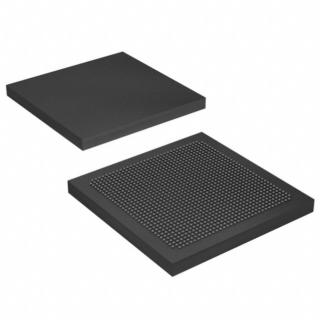
| Package / Case | 1152-BBGA, FCBGA | Number of I/O | 492 | Voltage | 870 mV - 980 mV | ||
| Mounting Method | Surface Mount | RoHS Compliance | RoHS Compliant | REACH Compliance | REACH Unaffected | ||
| Moisture Sensitivity Level | 3 (168 Hours) | Number of LABs/CLBs | 217080 | Number of Logic Elements/Cells | 570000 | ||
| Number of Gates | N/A | ECCN | 3A001A7B | HTS Code | 8542.39.0001 | ||
| Qualification | N/A | Total RAM Bits | 42082304 |
Overview of 10AX057H2F34I2LG – Arria 10 GX FPGA 1152‑FCBGA
The 10AX057H2F34I2LG is an Intel Arria 10 GX Field Programmable Gate Array (FPGA) supplied in a 1152‑ball FCBGA (35×35) surface‑mount package. It is a 20‑nm mid‑range, high‑performance, power‑efficient FPGA intended for applications across wireless, wireline, broadcast, computing, medical and defense markets.
Designed for complex, performance‑sensitive designs, the device integrates a large logic fabric, substantial embedded memory, broad I/O and support for hardened IP blocks described in the Arria 10 device family documentation to address demanding mid‑range system requirements.
Key Features
- Logic Capacity Approximately 570,000 logic elements to support complex digital designs and system integration.
- Embedded Memory 42,082,304 total RAM bits for on‑chip buffering, lookup tables and data storage.
- I/O Density 492 general purpose I/O pins to accommodate broad peripheral and interface requirements.
- Transceiver and IP Capabilities Arria 10 device family documentation references low‑power serial transceivers and hard IP including PCIe Gen1/Gen2/Gen3 and support for 10 Gbps Ethernet and Interlaken (as applicable to Arria 10 GX variants).
- DSP and Compute Blocks Variable‑precision DSP block architecture is part of the Arria 10 feature set for arithmetic‑intensive workloads.
- Clocking and Reconfiguration Comprehensive clock networks with PLL clock sources and support for dynamic and partial reconfiguration as documented for the Arria 10 family.
- Power and Supply Core voltage supply range: 870 mV to 980 mV to support optimized power delivery and device operation.
- Package & Mounting 1152‑FBGA (1152‑FCBGA, 35×35) surface‑mount package for board‑level integration.
- Environmental & Compliance Industrial grade device with operating temperature range of −40 °C to 100 °C and RoHS compliance.
Typical Applications
- Wireless Infrastructure Channel and switch cards in remote radio heads and mobile backhaul systems leveraging the device’s logic and transceiver capabilities.
- Wireline Networking 40G/100G muxponders, transponders and line cards where embedded memory and hardened protocol IP are required.
- Broadcast & Pro AV Studio switches, video transport and professional audio/video processing that benefit from large logic capacity and on‑chip memory.
- Computing & Storage Acceleration Flash cache, server acceleration and cloud compute functions using the device’s DSP and logic resources.
- Medical and Defense Systems Diagnostic imaging, radar, missile guidance and secure communications applications within the specified industrial temperature range.
Unique Advantages
- High integration density: 570,000 logic elements and extensive embedded memory enable consolidation of functions onto a single FPGA to reduce BOM and board area.
- Broad I/O and interface support: 492 I/O pins and Arria 10 family transceiver/IP support simplify connectivity to high‑speed links and external peripherals.
- Industrial temperature range: Rated for −40 °C to 100 °C, suitable for demanding environmental conditions.
- Optimized core power window: 0.87–0.98 V core supply range supports power delivery designs tuned for efficiency.
- Surface‑mount FCBGA package: 1152‑ball FCBGA (35×35) provides high pin density for complex system routing and thermal management on modern PCBs.
- Standards and compliance: RoHS compliance supports environmentally regulated product builds.
Why Choose 10AX057H2F34I2LG?
The 10AX057H2F34I2LG Arria 10 GX FPGA combines a large logic fabric, substantial on‑chip RAM and broad I/O in an industrial‑grade, surface‑mount FCBGA package. It is positioned for mid‑range systems that require a balance of performance and power efficiency and where flexible I/O and embedded resources are critical.
Engineers developing wireless, wireline, broadcast, compute/storage, medical or defense applications will find the device’s documented Arria 10 capabilities—such as DSP blocks, embedded memory structures, clocking options and hardened protocol IP—useful for building scalable, reliable solutions backed by Arria 10 family documentation and development resources.
If you would like pricing, availability or a formal quote for 10AX057H2F34I2LG, submit a request today to begin the procurement process or to discuss your application requirements with our team.


Date Founded: 1968
Headquarters: Santa Clara, California, USA
Employees: 130,000+
Revenue: $54.23 Billion
Certifications and Memberships: ISO9001:2015, ISO14001:2015, ISO17025:2017, ISO27001:2022, ISO45001:2018, ISO50001:2018


