
10AX057H2F34E2SG
| Part Description |
Arria 10 GX Field Programmable Gate Array (FPGA) IC 492 42082304 570000 1152-BBGA, FCBGA |
|---|---|
| Quantity | 910 Available (as of June 15, 2026) |

| Product Category | Field Programmable Gate Array (FPGA) |
|---|---|
| Manufacturer | Intel |
| Manufacturing Status | Active |
| Manufacturer Standard Lead Time | 12 Weeks |
| Datasheet |
Specifications & Environmental
| Device Package | 1152-FCBGA (35x35) | Grade | Extended | Operating Temperature | 0°C – 100°C | ||
|---|---|---|---|---|---|---|---|
| Package / Case | 1152-BBGA, FCBGA | Number of I/O | 492 | Voltage | 870 mV - 980 mV | ||
| Mounting Method | Surface Mount | RoHS Compliance | RoHS Compliant | REACH Compliance | REACH Unaffected | ||
| Moisture Sensitivity Level | 3 (168 Hours) | Number of LABs/CLBs | 217080 | Number of Logic Elements/Cells | 570000 | ||
| Number of Gates | N/A | ECCN | 3A001A7B | HTS Code | 8542.39.0001 | ||
| Qualification | N/A | Total RAM Bits | 42082304 |
Overview of 10AX057H2F34E2SG – Arria 10 GX Field Programmable Gate Array (FPGA) IC
The 10AX057H2F34E2SG is an Intel Arria 10 GX field programmable gate array (FPGA) in a 1152‑FBGA package intended for mid-range, high-performance and power-efficient designs. It is built on a 20 nm process and targets applications that require substantial logic density, on-chip memory, and a large number of I/O connections.
Typical markets include wireless and wireline communications, broadcast, computing and storage, medical imaging, and defense applications where performance and power efficiency are key considerations.
Key Features
- Core Logic — 570,000 logic elements provide high logic density for complex digital designs.
- Logic Array Blocks — 217,080 reported logic array resources for fine-grained logic implementation and partitioning.
- On-chip Memory — 42,082,304 total RAM bits to support buffering, caching, and on-chip data storage for large designs.
- I/O Capacity — 492 user I/O pins to support broad connectivity to external devices and memory interfaces.
- Power Supply — Core supply range 870 mV to 980 mV for power planning and regulator selection.
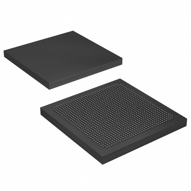
- Package & Mounting — 1152-FCBGA (35 × 35 mm) supplier package / 1152-BBGA package case, surface-mount for compact board integration.
- Thermal & Grade — Extended grade with an operating temperature range of 0 °C to 100 °C suitable for demanding commercial and industrial-adjacent environments.
- Standards & Compliance — RoHS compliant for environmental regulatory requirements.
Typical Applications
- Wireless Infrastructure — Channel and switch cards in remote radio heads and mobile backhaul systems leveraging high logic density and large on-chip RAM for signal processing.
- Wireline Networking — 40G/100G muxponders, transponders and line-card applications where programmable logic and extensive I/O enable protocol handling and data aggregation.
- Broadcast & Media — Studio switches, transport and professional audio/video processing that benefit from large memory and configurable logic for video/frame buffering and format conversion.
- Computing & Storage — Server acceleration, flash cache and cloud computing tasks that require scalable logic resources and on-chip memory for data path acceleration.
- Medical & Defense Systems — Diagnostic imaging, radar and secure communications where configurable logic, memory capacity, and robust I/O support application-specific processing.
Unique Advantages
- High logic density: 570,000 logic elements enable implementation of large, complex designs without partitioning across multiple devices.
- Substantial embedded memory: Over 42 million RAM bits support large buffers, caches, and state storage directly on chip to reduce external memory dependency.
- Extensive I/O: 492 I/O pins provide flexibility for wide parallel interfaces, multi-channel connectivity, and high-speed external memory interfaces.
- Compact advanced package: 1152‑FBGA (35 × 35 mm) packaging delivers a dense footprint for space-constrained boards while supporting high pin counts.
- Designed for performance and efficiency: Built on a 20 nm process with a tightly defined core voltage range to support performance-oriented power design.
- Regulatory readiness: RoHS compliance supports environmental requirements for commercial and industrial products.
Why Choose 10AX057H2F34E2SG?
The 10AX057H2F34E2SG Arria 10 GX FPGA combines high logic capacity, large on-chip RAM, and broad I/O in a compact 1152‑FBGA package, positioning it for mid-range applications that need a balance of performance and power efficiency. Its extended-grade thermal range and RoHS compliance make it suitable for demanding commercial and specialized applications across communications, broadcast, computing, medical, and defense markets.
Designers seeking a scalable, programmable platform with substantial on-chip resources and flexible connectivity will find this device appropriate for accelerating development cycles and consolidating functions that would otherwise require multiple components.
Request a quote or submit an inquiry to check availability, pricing, and lead times for the 10AX057H2F34E2SG Arria 10 GX FPGA.


Date Founded: 1968
Headquarters: Santa Clara, California, USA
Employees: 130,000+
Revenue: $54.23 Billion
Certifications and Memberships: ISO9001:2015, ISO14001:2015, ISO17025:2017, ISO27001:2022, ISO45001:2018, ISO50001:2018


