
10AX057H2F34E1HG
| Part Description |
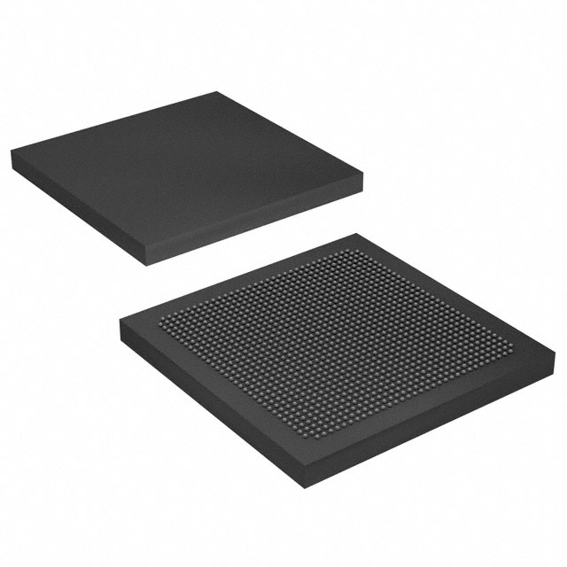
Arria 10 GX Field Programmable Gate Array (FPGA) IC 492 42082304 570000 1152-BBGA, FCBGA |
|---|---|
| Quantity | 389 Available (as of June 18, 2026) |
| Product Category | Field Programmable Gate Array (FPGA) |
|---|---|
| Manufacturer | Intel |
| Manufacturing Status | Active |
| Manufacturer Standard Lead Time | 16 Weeks |
| Datasheet |
Specifications & Environmental
| Device Package | 1152-FCBGA (35x35) | Grade | Extended | Operating Temperature | 0°C – 100°C | ||
|---|---|---|---|---|---|---|---|
| Package / Case | 1152-BBGA, FCBGA | Number of I/O | 492 | Voltage | 870 mV - 980 mV | ||
| Mounting Method | Surface Mount | RoHS Compliance | RoHS Compliant | REACH Compliance | REACH Unaffected | ||
| Moisture Sensitivity Level | 3 (168 Hours) | Number of LABs/CLBs | 217080 | Number of Logic Elements/Cells | 570000 | ||
| Number of Gates | N/A | ECCN | 5A002A1 | HTS Code | 8542.39.0001 | ||
| Qualification | N/A | Total RAM Bits | 42082304 |
Overview of 10AX057H2F34E1HG – Arria 10 GX FPGA, 570,000 Logic Elements, 1152‑FCBGA
The 10AX057H2F34E1HG is an Intel Arria 10 GX field programmable gate array (FPGA) optimized for high‑performance, power‑efficient midrange applications. It combines a high logic count, substantial embedded memory, and a broad I/O complement in a 1152‑FCBGA (35×35) surface‑mount package for system designs that require a balance of density, integration, and power efficiency.
Arria 10 devices target markets such as wireless and wireline communications, broadcast, computing and storage, medical imaging, and defense. This device is positioned for applications that benefit from large programmable logic capacity, extensive on‑chip RAM, flexible clocking and transceiver options, and extended temperature operation.
Key Features
- High logic capacity — 570,000 logic elements to support complex algorithms, wide datapaths, and large custom logic implementations.
- Substantial embedded memory — 42,082,304 total RAM bits of on‑chip memory for buffering, caching, and high‑throughput data paths.
- Extensive I/O — 492 I/O pins to interface with diverse peripherals, memory devices, and high‑speed interfaces.
- Adaptive logic and DSP — Device architecture includes adaptive logic modules and variable‑precision DSP blocks for compute‑intensive signal processing and algorithm acceleration.
- Transceivers and high‑speed IP — Arria 10 family features low‑power serial transceivers, enhanced PCS hard IP, and PCIe hard IP options suitable for high‑bandwidth links (series‑level feature referenced in product documentation).
- Clocking and PLLs — Robust clock networks with fractional synthesis and I/O PLLs enable flexible timing architectures and multiple clock domain management.
- Package and mounting — 1152‑FCBGA (35×35) surface‑mount package tailored for board‑level assembly with a compact footprint.
- Power and supply — Core voltage supply range of 870 mV to 980 mV to support targeted power profiles.
- Extended temperature grade — Rated for 0 °C to 100 °C operation for applications requiring broadened commercial/extended temperature operation.
- RoHS compliant — Conforms to RoHS requirements for environmental compliance.
Typical Applications
- Wireless infrastructure — Channel processing and switch cards in remote radio heads and mobile backhaul equipment that require high logic density and DSP capabilities.
- Wireline and transport — 40G/100G muxponders, transponders, and line cards where high‑speed transceivers and hardened IP blocks support aggregation and bridging functions.
- Broadcast and professional video — Studio switches, transport, and videoconferencing systems leveraging large on‑chip memory and dense logic for real‑time media processing.
- Computing and storage — Server acceleration, flash cache, and cloud computing infrastructure requiring hardware acceleration and extensive I/O connectivity.
- Medical and defense systems — Diagnostic imaging, radar, and electronic warfare subsystems that benefit from programmable acceleration and robust clocking and I/O resources.
Unique Advantages
- High integration density: 570,000 logic elements enable complex system functions to be consolidated into a single FPGA, reducing board‑level component count.
- Large on‑chip memory: Over 42 million RAM bits provide ample capacity for buffering, packet processing, and data‑intensive algorithms without immediate external memory dependence.
- Broad I/O and connectivity: 492 I/Os and family‑level transceiver/IP options support diverse peripherals and high‑bandwidth links for modern communication systems.
- Flexible timing and DSP support: Adaptive logic modules, variable‑precision DSP blocks, and comprehensive PLLs support mixed‑signal timing domains and high‑performance signal processing chains.
- Compact, manufacturable package: 1152‑FCBGA (35×35) surface‑mount package balances density with assembly suitability for production environments.
- Extended operating range and compliance: 0 °C to 100 °C rating and RoHS compliance help meet environmental and regulatory requirements for a wide set of deployments.
Why Choose 10AX057H2F34E1HG?
The 10AX057H2F34E1HG Arria 10 GX FPGA delivers a combination of high logic density, large embedded memory, and extensive I/O in a single, surface‑mount 1152‑FCBGA package. It is well suited for midrange designs that demand a balance of compute capability, power efficiency, and flexible connectivity—particularly in communications, broadcast, compute acceleration, and imaging applications.
Backed by Intel Arria 10 device documentation and family resources, this device is a practical choice for engineers seeking a scalable FPGA fabric with robust clocking, DSP, and transceiver options, enabling long‑term design scalability and integration into complex system architectures.
Request a quote or submit an inquiry for pricing and availability to evaluate the 10AX057H2F34E1HG for your next design.


Date Founded: 1968
Headquarters: Santa Clara, California, USA
Employees: 130,000+
Revenue: $54.23 Billion
Certifications and Memberships: ISO9001:2015, ISO14001:2015, ISO17025:2017, ISO27001:2022, ISO45001:2018, ISO50001:2018


