
10AX057K3F35E2SG
| Part Description |
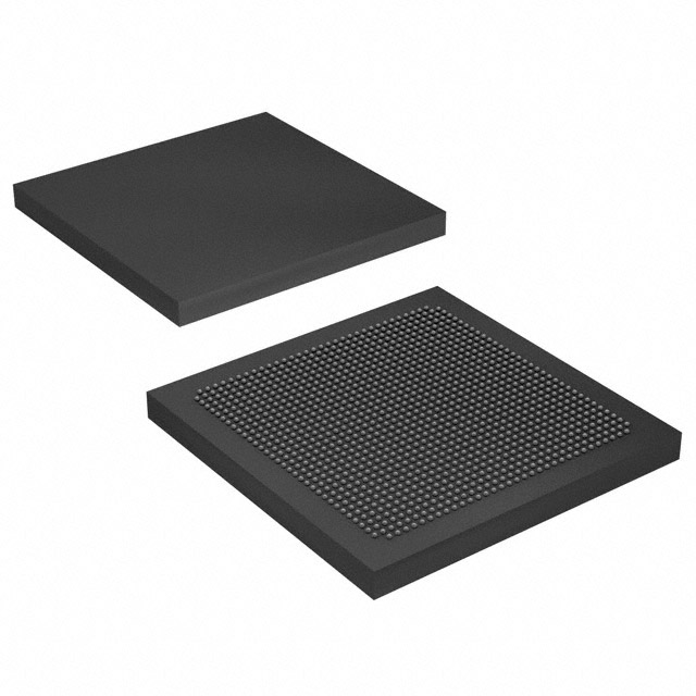
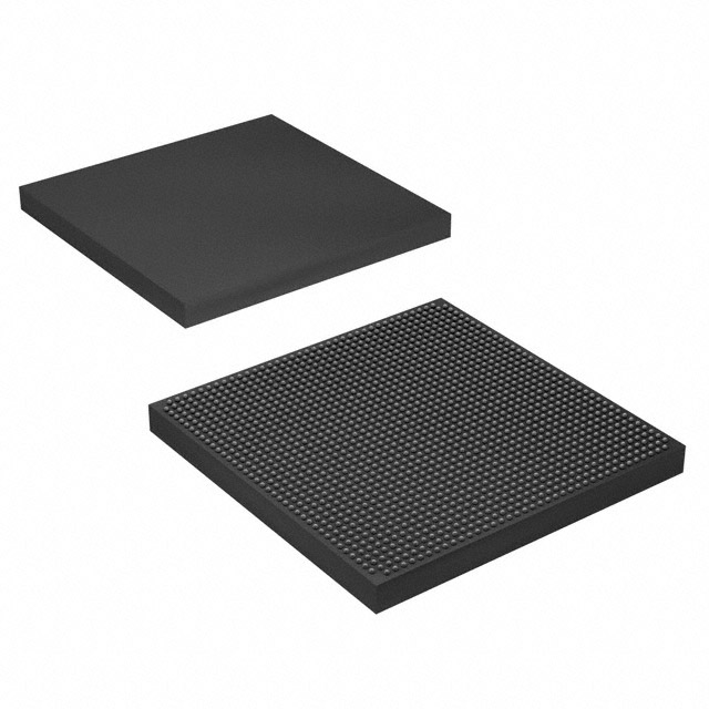
Arria 10 GX Field Programmable Gate Array (FPGA) IC 396 42082304 570000 1152-BBGA, FCBGA |
|---|---|
| Quantity | 505 Available (as of October 8, 2026) |
| Product Category | Field Programmable Gate Array (FPGA) |
|---|---|
| Manufacturer | Intel |
| Manufacturing Status | Active |
| Manufacturer Standard Lead Time | 12 Weeks |
| Datasheet |
Specifications & Environmental
| Device Package | 1152-FCBGA (35x35) | Grade | Extended | Operating Temperature | 0°C – 100°C | ||
|---|---|---|---|---|---|---|---|
| Package / Case | 1152-BBGA, FCBGA | Number of I/O | 396 | Voltage | 870 mV - 930 mV | ||
| Mounting Method | Surface Mount | RoHS Compliance | RoHS Compliant | REACH Compliance | REACH Unaffected | ||
| Moisture Sensitivity Level | 3 (168 Hours) | Number of LABs/CLBs | 217080 | Number of Logic Elements/Cells | 570000 | ||
| Number of Gates | N/A | ECCN | 3A001A7B | HTS Code | 8542.39.0001 | ||
| Qualification | N/A | Total RAM Bits | 42082304 |
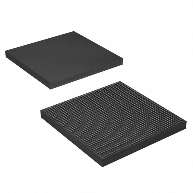
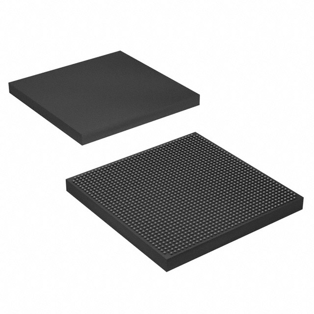
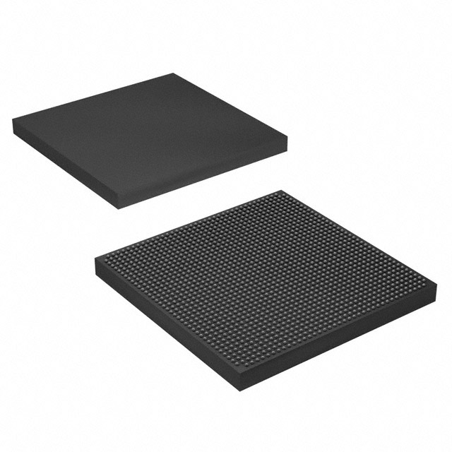
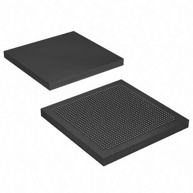
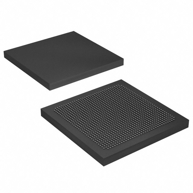
Overview of 10AX057K3F35E2SG – Arria 10 GX FPGA, 570,000 logic elements, 42,082,304 RAM bits, 396 I/O, 1152‑FCBGA (35×35)
The 10AX057K3F35E2SG is an Intel Arria 10 GX Field Programmable Gate Array (FPGA) IC designed for mid-range, performance-sensitive applications. Built on the Arria 10 device family architecture, this part combines a large programmable fabric with significant on‑chip memory and a high I/O count to support complex digital logic and data buffering on a single device.
Targeted at markets including wireless, wireline, broadcast, computing and storage, and other mid-range systems, the device delivers the family’s stated focus on higher performance and power efficiency in a 20‑nm FPGA architecture.
Key Features
- Programmable Fabric (Logic) 570,000 logic elements provide a large, flexible logic resource for implementing custom datapaths, controllers, and accelerators.
- Embedded Memory Total on‑chip RAM capacity of 42,082,304 bits supports buffering, caching, and temporary storage for high‑throughput designs.
- I/O Density 396 I/O pins enable extensive board‑level connectivity for parallel interfaces, memory buses, and mixed external peripherals.
- Package 1152‑FCBGA package (35×35 mm) offers a high pin‑count footprint suitable for dense board layouts with surface‑mount assembly.
- Power and Voltage Core voltage supply specified from 870 mV to 930 mV to support the device’s operating requirements.
- Operating Range & Grade Extended grade with an operating temperature range of 0 °C to 100 °C for broader ambient conditions.
- Mounting and Compliance Surface mount device; RoHS compliant for lead‑free manufacturing processes.
- Arria 10 Family Characteristics Part of the 20‑nm Arria 10 family, which emphasizes higher performance and power efficiency for mid‑range FPGA and SoC applications.
Typical Applications
- Wireless Infrastructure Channel and switch cards in remote radio heads and mobile backhaul systems where programmable logic and on‑chip memory accelerate signal processing.
- Wireline Networking Muxponder, transponder and line‑card functions in 40G/100G systems that require dense logic and high I/O connectivity.
- Broadcast & Pro AV Studio switching and professional audio/video transport where flexible data routing and buffering are needed.
- Computing & Storage Server acceleration, flash cache and cloud compute tasks that leverage large logic resources and on‑chip memory for throughput optimization.
- Medical & Defense Diagnostic imaging, radar, and secure communications applications that use programmable hardware for specialized processing and control.
Unique Advantages
- Large, Integrated Fabric: 570,000 logic elements enable complex system integration on a single FPGA, reducing external component count.
- Substantial On‑Chip Memory: 42,082,304 RAM bits provide meaningful capacity for buffering and local data handling without immediate reliance on external memory.
- High I/O Count: 396 I/O pins accommodate wide bus interfaces and multiple peripherals, simplifying board‑level connectivity.
- Compact High‑Pin Package: 1152‑FCBGA (35×35) packs high pin density into a manufacturable surface‑mount form factor for space‑constrained designs.
- Designed for Mid‑Range Performance: As part of the Arria 10 family, the device targets higher performance and power efficiency within the 20‑nm mid‑range FPGA segment.
- Extended Operating Range: Extended grade and 0 °C to 100 °C operation support deployment in a variety of ambient environments.
Why Choose 10AX057K3F35E2SG?
The 10AX057K3F35E2SG positions itself for designs that require a substantial combination of programmable logic, embedded memory, and high I/O density in a single FPGA. Its placement in the Intel Arria 10 family aligns the device with a 20‑nm architecture focused on delivering higher performance and improved power efficiency for mid‑range applications.
This part is suitable for engineering teams building wireless, wireline, broadcast, computing, medical, and defense systems that benefit from on‑device logic and memory consolidation, a compact high‑pin package, and extended operating temperature support. The device’s feature set aims to simplify board design while providing the resources needed for complex custom functions.
Request a quote or submit a pricing inquiry today to check availability and receive detailed ordering information for 10AX057K3F35E2SG.





















Date Founded: 1968
Headquarters: Santa Clara, California, USA
Employees: 130,000+
Revenue: $54.23 Billion
Certifications and Memberships: ISO9001:2015, ISO14001:2015, ISO17025:2017, ISO27001:2022, ISO45001:2018, ISO50001:2018


