
10AX066N1F40E1HG
| Part Description |
Arria 10 GX Field Programmable Gate Array (FPGA) IC 588 49610752 660000 1517-BBGA, FCBGA |
|---|---|
| Quantity | 92 Available (as of June 14, 2026) |

| Product Category | Field Programmable Gate Array (FPGA) |
|---|---|
| Manufacturer | Intel |
| Manufacturing Status | Active |
| Manufacturer Standard Lead Time | 12 Weeks |
| Datasheet |
Specifications & Environmental
| Device Package | 1517-FBGA (40x40) | Grade | Extended | Operating Temperature | 0°C – 100°C | ||
|---|---|---|---|---|---|---|---|
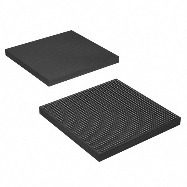
| Package / Case | 1517-BBGA, FCBGA | Number of I/O | 588 | Voltage | 870 mV - 980 mV | ||
| Mounting Method | Surface Mount | RoHS Compliance | RoHS Compliant | REACH Compliance | REACH Unaffected | ||
| Moisture Sensitivity Level | 3 (168 Hours) | Number of LABs/CLBs | 250540 | Number of Logic Elements/Cells | 660000 | ||
| Number of Gates | N/A | ECCN | 5A002A1 | HTS Code | 8542.39.0001 | ||
| Qualification | N/A | Total RAM Bits | 49610752 |
Overview of 10AX066N1F40E1HG – Arria 10 GX FPGA, 660,000 logic elements, 49,610,752-bit RAM, 588 I/Os
The 10AX066N1F40E1HG is an Intel Arria 10 GX field programmable gate array (FPGA) packaged in a 1517-BBGA (1517-FBGA, 40×40) FCBGA offering high logic density and large embedded memory. It targets mid-range, high-performance, power-sensitive applications.
As part of the Arria 10 device family, this FPGA delivers higher performance than the previous generation and incorporates power-efficiency technologies. Typical markets include wireless and wireline infrastructure, broadcast, computing and storage, medical imaging, and defense communications.
Key Features
- Programmable Logic 660,000 logic elements provide the programmable fabric for complex digital designs and custom accelerators.
- Embedded Memory Total embedded RAM capacity of 49,610,752 bits supports large on-chip buffering and memory-intensive functions.
- I/O Capability 588 I/Os enable extensive external interfacing and flexible board-level connectivity.
- Transceivers and High-Speed Interfaces Arria 10 GX device family includes low-power serial transceivers, PCS/PMA features, and hard IP for high-speed protocols referenced in the device overview.
- Hard IP and Interfaces Device overview documents PCIe Gen1/Gen2/Gen3 hard IP, enhanced PCS hard IP for Interlaken and 10 Gbps Ethernet, and external memory interface support.
- Clocking and PLLs Comprehensive clock networks with fractional synthesis and I/O PLLs for flexible timing architectures, as described in the device documentation.
- Power and Supply Operates from an internal voltage supply range of 870 mV to 980 mV, with power-efficiency features indicated for the Arria 10 family.
- Package and Mounting 1517-BBGA (supplier package: 1517-FBGA, 40×40) FCBGA, surface-mount mounting type for compact board designs.
- Operating Range and Grade Extended-grade device with an operating temperature range of 0 °C to 100 °C.
- RoHS Compliant Environmentally compliant with RoHS requirements.
Typical Applications
- Wireless Infrastructure Channel and switch cards in remote radio heads and mobile backhaul systems leveraging the device's programmable fabric and transceiver capabilities.
- Wireline Networking 40G/100G muxponders, transponders, and 100G line cards that use the device's high-speed interfaces and hard IP for protocol handling.
- Broadcast and Media Studio switches, servers, and transport systems for video and audio processing requiring large embedded memory and flexible I/O.
- Computing and Storage Flash cache, cloud computing servers, and server acceleration functions that benefit from high logic density and on-chip RAM.
- Medical and Defense Systems Diagnostic imaging, radar, and secure communications where the device family's performance and power-efficiency are advantageous.
Unique Advantages
- High Logic Density: 660,000 logic elements enable integration of complex digital functions and system-level consolidation on a single FPGA.
- Significant On-Chip Memory: Nearly 50 Mbits of embedded RAM reduce reliance on external memory for buffering and accelerators, simplifying board-level design.
- Comprehensive High-Speed Connectivity: Arria 10 GX family features low-power serial transceivers and hard IP for PCIe and high-speed Ethernet protocols, accelerating interface development.
- Flexible Clocking and Timing: Advanced clock networks and PLL options support diverse timing architectures and fractional synthesis for precision clocking.
- Compact, Surface-Mount Packaging: 1517-BBGA FCBGA package (1517-FBGA, 40×40) supports high I/O count in a compact footprint for dense board layouts.
- Proven Device Family: Part of the Intel Arria 10 family, which emphasizes improved performance and power efficiency over previous generations and is supported by device documentation for development.
Why Choose 10AX066N1F40E1HG?
This Arria 10 GX FPGA balances high logic density, substantial on-chip memory, and extensive I/O to address mid-range, performance-sensitive designs that also demand energy efficiency. Its feature set—documented transceivers, hard IP for common protocols, and flexible clocking—helps accelerate development of networking, broadcast, compute, and imaging systems.
Engineers selecting 10AX066N1F40E1HG gain a solution positioned for scalability and integration within the Arria 10 family, backed by Intel's device documentation and design resources. The package, supply range, and extended operating grade make it suitable for demanding board-level implementations while meeting RoHS compliance.
Request a quote or submit an RFQ to receive pricing and availability information for 10AX066N1F40E1HG.


Date Founded: 1968
Headquarters: Santa Clara, California, USA
Employees: 130,000+
Revenue: $54.23 Billion
Certifications and Memberships: ISO9001:2015, ISO14001:2015, ISO17025:2017, ISO27001:2022, ISO45001:2018, ISO50001:2018


