
10AX066N1F40E1SG
| Part Description |
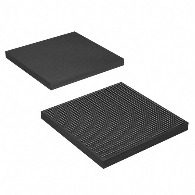
Arria 10 GX Field Programmable Gate Array (FPGA) IC 588 49610752 660000 1517-BBGA, FCBGA |
|---|---|
| Quantity | 209 Available (as of June 14, 2026) |

| Product Category | Field Programmable Gate Array (FPGA) |
|---|---|
| Manufacturer | Intel |
| Manufacturing Status | Discontinued |
| Manufacturer Standard Lead Time | 13 Weeks |
| Datasheet |
Specifications & Environmental
| Device Package | 1517-FCBGA (40x40) | Grade | Extended | Operating Temperature | 0°C – 100°C | ||
|---|---|---|---|---|---|---|---|
| Package / Case | 1517-BBGA, FCBGA | Number of I/O | 588 | Voltage | 870 mV - 980 mV | ||
| Mounting Method | Surface Mount | RoHS Compliance | RoHS Compliant | REACH Compliance | REACH Unaffected | ||
| Moisture Sensitivity Level | 3 (168 Hours) | Number of LABs/CLBs | 250540 | Number of Logic Elements/Cells | 660000 | ||
| Number of Gates | N/A | ECCN | 3A001A7B | HTS Code | 8542.39.0001 | ||
| Qualification | N/A | Total RAM Bits | 49610752 |
Overview of 10AX066N1F40E1SG – Arria 10 GX FPGA (1517-FCBGA)
The 10AX066N1F40E1SG is an Intel Arria 10 GX field‑programmable gate array (FPGA) supplied in a 1517‑ball FCBGA (40×40) package. As a member of the Arria 10 family, this device targets high‑performance, power‑sensitive midrange applications across communications, broadcast, computing, medical, and defense markets.
Designed for integration-heavy designs, the device combines substantial programmable logic capacity, large embedded RAM, and a wide I/O complement to enable complex system functions while supporting low‑voltage operation and extended temperature use. It is RoHS‑compliant.
Key Features
- Logic Capacity — 660,000 logic elements to implement large, complex digital functions and custom hardware accelerators.
- Embedded Memory — 49,610,752 total RAM bits for on‑chip buffering, frame storage, and data‑path memory requirements.
- I/O — 588 user I/O pins to support multiple external interfaces and parallel connectivity.
- Package — 1517‑FBCA (1517‑FCBGA, 40×40) package for high‑density board integration and thermal conduction.
- Power — Supported core voltage range from 870 mV to 980 mV, enabling designs that target low‑voltage power domains.
- Operating Temperature — Rated for 0 °C to 100 °C operation (Extended grade), suitable for many commercial and enterprise environments.
- Standards & Family Features — Part of the Intel Arria 10 family, which includes device features such as variable‑precision DSP blocks, embedded memory architectures, clock networks and PLLs, and hard IP options for common interfaces as described in Intel Arria 10 documentation.
- Compliance — RoHS compliant for environmental regulatory alignment.
Typical Applications
- Wireless Infrastructure — Channel and switch cards, remote radio head functions, and mobile backhaul equipment benefiting from programmable logic and high I/O density.
- Wireline & Networking — Line cards, muxponders, and transponder functions where on‑chip memory and logic capacity accelerate packet processing and protocol handling.
- Broadcast & Media — Studio switches, video transport, and professional audio/video processing that require large RAM capacity and flexible I/O.
- Computing & Storage — Server acceleration, flash cache controllers, and cloud computing components that leverage FPGA logic for offload and custom data paths.
- Medical & Defense Systems — Diagnostic imaging, radar, and communications equipment that benefit from programmable algorithms and the Arria 10 family’s power‑performance orientation.
Unique Advantages
- High Logic Density: 660,000 logic elements provide the headroom to implement complex finite state machines, accelerators, and custom datapaths on a single device.
- Large On‑Chip Memory: Nearly 50 Mbit of embedded RAM supports buffer‑intensive applications such as video processing, packet buffering, and caching.
- Extensive I/O Availability: 588 I/O pins simplify interfacing to external memories, PHYs, and system peripherals without excessive board-level multiplexing.
- Low‑Voltage Core Operation: Core voltage support from 870 mV to 980 mV enables integration into modern low‑power system domains.
- Extended Grade Packaging: The device’s extended operating temperature range (0 °C to 100 °C) and FCBGA packaging support deployment in a wide range of commercial and enterprise systems.
- Part of Arria 10 Ecosystem: Being an Arria 10 device means access to family documentation and device‑level features such as DSP blocks, PLLs, and embedded memory architectures referenced in the Arria 10 overview materials.
Why Choose 10AX066N1F40E1SG?
The 10AX066N1F40E1SG positions itself for midrange designs that need a balance of logic capacity, on‑chip memory, and robust I/O in a single, low‑voltage FPGA package. Its place within the Intel Arria 10 family aligns this part with device‑level features and documentation oriented toward power‑sensitive, high‑performance applications.
For engineers and procurement professionals designing communications, compute acceleration, broadcast, or imaging systems, this Arria 10 GX device offers a measurable combination of programmable logic, embedded RAM, and I/O resources that support scalable designs and long‑term platform evolution.
Request a quote or submit an inquiry to learn about availability, pricing, and lead times for the 10AX066N1F40E1SG Arria 10 GX FPGA.


Date Founded: 1968
Headquarters: Santa Clara, California, USA
Employees: 130,000+
Revenue: $54.23 Billion
Certifications and Memberships: ISO9001:2015, ISO14001:2015, ISO17025:2017, ISO27001:2022, ISO45001:2018, ISO50001:2018


