
10AX090S2F45E1SG
| Part Description |
Arria 10 GX Field Programmable Gate Array (FPGA) IC 624 59234304 900000 1932-BBGA, FCBGA |
|---|---|
| Quantity | 931 Available (as of June 18, 2026) |

| Product Category | Field Programmable Gate Array (FPGA) |
|---|---|
| Manufacturer | Intel |
| Manufacturing Status | Active |
| Manufacturer Standard Lead Time | 16 Weeks |
| Datasheet |
Specifications & Environmental
| Device Package | 1932-FCBGA (45x45) | Grade | Extended | Operating Temperature | 0°C – 100°C | ||
|---|---|---|---|---|---|---|---|
| Package / Case | 1932-BBGA, FCBGA | Number of I/O | 624 | Voltage | 870 mV - 980 mV | ||
| Mounting Method | Surface Mount | RoHS Compliance | RoHS Compliant | REACH Compliance | REACH Unaffected | ||
| Moisture Sensitivity Level | 3 (168 Hours) | Number of LABs/CLBs | 339620 | Number of Logic Elements/Cells | 900000 | ||
| Number of Gates | N/A | ECCN | 3A001A7A | HTS Code | 8542.39.0001 | ||
| Qualification | N/A | Total RAM Bits | 59234304 |
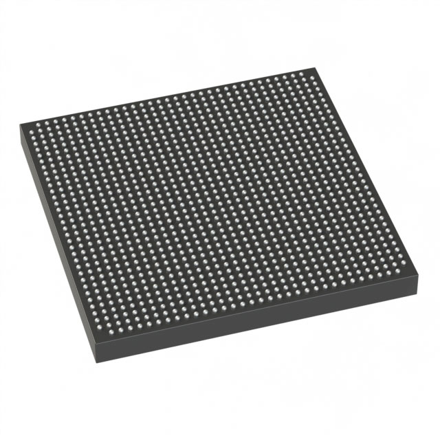
Overview of 10AX090S2F45E1SG – Arria 10 GX FPGA, 900,000 logic elements, 1932-FCBGA
The 10AX090S2F45E1SG is an Intel Arria 10 GX field-programmable gate array (FPGA) supplied in a 1932-FCBGA (45×45) package. It delivers a high-capacity, mid-range programmable fabric with an emphasis on performance and power efficiency for demanding embedded and communications applications.
Designed for markets such as wireless, wireline, broadcast, computing and military systems, this device combines large logic and memory resources with extensive I/O and advanced serial/PCIe hard IP to support complex, high-throughput designs.
Key Features
- Programmable Fabric — 900,000 logic elements provide substantial capacity for complex logic, control and acceleration tasks.
- Embedded Memory — 59,234,304 total RAM bits to support large buffering, packet processing and on-chip data storage.
- High I/O Count — 624 I/O pins for flexible interfacing to high-speed memory, PHYs, and system peripherals.
- Transceivers and High-Speed Interfaces — Arria 10 GX features low-power serial transceivers, enhanced PCS Hard IP for Interlaken and 10 Gbps Ethernet, and PCIe Gen1/Gen2/Gen3 Hard IP for high-bandwidth link integration.
- DSP and Clocking — Variable-precision DSP blocks for arithmetic-intensive processing and comprehensive clock networks with fractional synthesis and I/O PLLs.
- Package, Power and Thermal — 1932-FCBGA (45×45) surface-mount package; supply voltage range 870 mV to 980 mV; operating temperature 0 °C to 100 °C; Extended grade.
- Compliance and Documentation — RoHS compliant and supported by Intel device documentation including device overview and handbook references.
Typical Applications
- Wireless infrastructure — Channel and switch cards in remote radio heads and mobile backhaul systems where FPGA-based signal processing and protocol handling are required.
- Wireline optics and switching — 40G/100G muxponders, transponders and 100G line cards that need high-throughput packet processing and protocol offload.
- Broadcast and professional AV — Studio switches and transport equipment that require low-latency processing and flexible signal routing.
- Computing and storage acceleration — Flash cache, cloud server acceleration and compute offload where large on-chip memory and DSP resources improve throughput and latency.
- Defense and secure communications — Radar, electronic warfare, missile guidance and secure link processing that demand configurable logic and high-speed serial interfaces.
Unique Advantages
- High integration density: 900,000 logic elements combined with 59,234,304 RAM bits and 624 I/Os reduce external component count and simplify system architecture.
- Advanced connectivity: Built-in support for PCIe Gen1/2/3 Hard IP, Interlaken and 10 Gbps Ethernet along with low-power transceivers enables straightforward integration of high-bandwidth links.
- Flexible signal processing: Variable-precision DSP blocks and large on-chip memory make the device suitable for compute-heavy signal-processing tasks.
- Power-aware mid-range performance: Part of the 20 nm Arria 10 family that emphasizes performance with power-efficiency features, suitable for power-sensitive designs.
- Compact, manufacturable package: 1932-FCBGA (45×45) surface-mount package supports dense PCB layouts while meeting extended-grade thermal and supply conditions.
- Documented support: Backed by Intel device documentation and design resources for development guidance and system integration.
Why Choose 10AX090S2F45E1SG?
The 10AX090S2F45E1SG positions itself as a high-capacity, power-conscious mid-range FPGA for applications that require large programmable logic, substantial embedded memory, and extensive I/O and high-speed serial interfaces. Its Arria 10 GX lineage provides architectural features—such as DSP blocks, advanced clocking, and hardened interface IP—that accelerate time-to-market for complex communications, broadcast, compute and defense systems.
This device is suited for engineers and system designers who need a balanced combination of logic density, on-chip memory, and connectivity while maintaining power efficiency and manufacturing readiness with an Extended grade surface-mount FCBGA package.
Request a quote or submit a quote for pricing and availability.


Date Founded: 1968
Headquarters: Santa Clara, California, USA
Employees: 130,000+
Revenue: $54.23 Billion
Certifications and Memberships: ISO9001:2015, ISO14001:2015, ISO17025:2017, ISO27001:2022, ISO45001:2018, ISO50001:2018


