
10AX090S2F45I2LG
| Part Description |
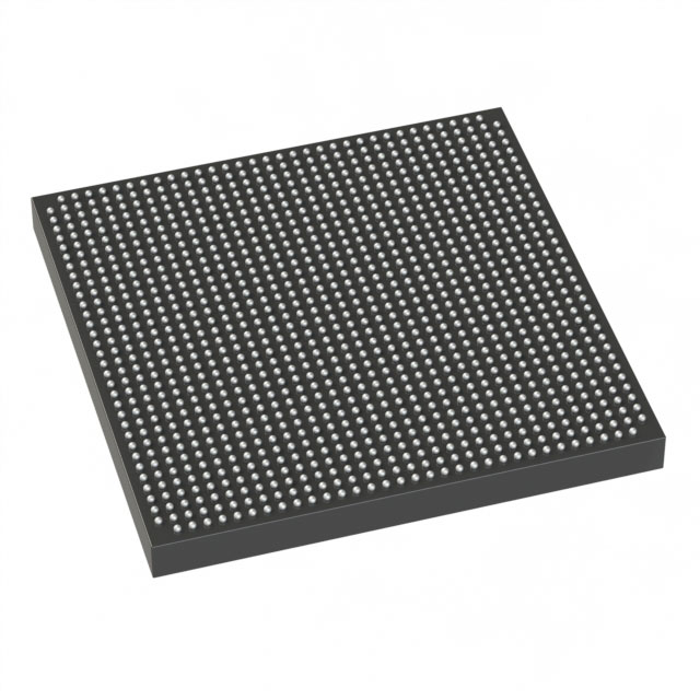
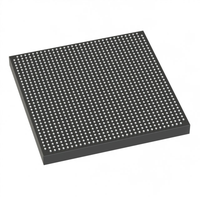
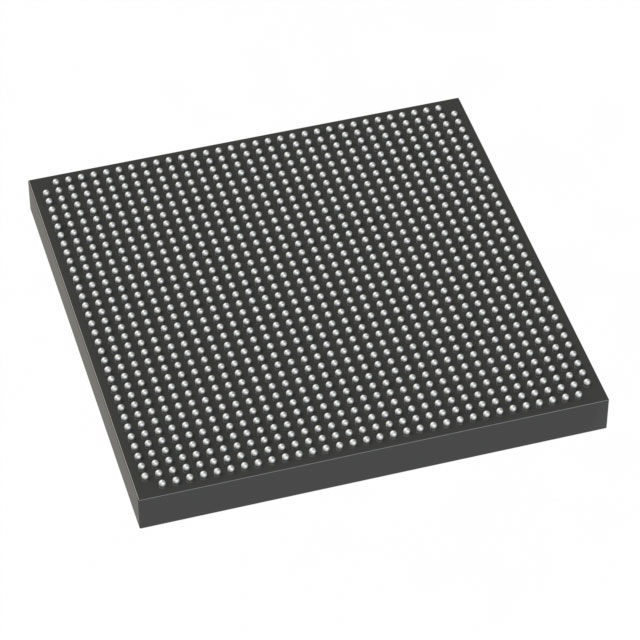
Arria 10 GX Field Programmable Gate Array (FPGA) IC 624 59234304 900000 1932-BBGA, FCBGA |
|---|---|
| Quantity | 475 Available (as of October 8, 2026) |
| Product Category | Field Programmable Gate Array (FPGA) |
|---|---|
| Manufacturer | Intel |
| Manufacturing Status | Active |
| Manufacturer Standard Lead Time | 16 Weeks |
| Datasheet |
Specifications & Environmental
| Device Package | 1932-FCBGA (45x45) | Grade | Industrial | Operating Temperature | -40°C – 100°C | ||
|---|---|---|---|---|---|---|---|
| Package / Case | 1932-BBGA, FCBGA | Number of I/O | 624 | Voltage | 870 mV - 980 mV | ||
| Mounting Method | Surface Mount | RoHS Compliance | RoHS Compliant | REACH Compliance | REACH Unaffected | ||
| Moisture Sensitivity Level | 3 (168 Hours) | Number of LABs/CLBs | 339620 | Number of Logic Elements/Cells | 900000 | ||
| Number of Gates | N/A | ECCN | 3A001A7A | HTS Code | 8542.39.0001 | ||
| Qualification | N/A | Total RAM Bits | 59234304 |
Overview of 10AX090S2F45I2LG – Arria 10 GX FPGA, 900,000 Logic Elements, 1932-FCBGA
The 10AX090S2F45I2LG is an Intel Arria 10 GX field programmable gate array (FPGA) in a 1932-ball FCBGA package. It is a 20 nm mid-range, high-performance FPGA offering large logic capacity and on‑chip memory targeted at demanding communications, compute and industrial applications.
With 900,000 logic elements and over 59 million bits of embedded RAM, this device is designed for applications that require high I/O density, significant on‑chip memory bandwidth, and operation across an industrial temperature range.
Key Features
- Logic Capacity 900,000 logic elements provide substantial programmable fabric for complex logic, control and signal-processing tasks.
- Embedded Memory 59,234,304 total RAM bits enable large on‑chip storage for buffering, packet processing, and lookup tables.
- I/O Density 624 user I/O pins support high‑density external interfacing for multi‑lane links, memory interfaces, and board-level connectivity.
- Transceiver and Series Architecture (Arria 10 GX) Part of the Arria 10 GX family, offering device-level features and architecture for mid-range FPGA applications described in the device overview.
- Power Supply Range Core voltage operation between 870 mV and 980 mV for defined power delivery and regulator selection.
- Industrial Temperature Rating Qualified for operation from −40 °C to 100 °C for deployment in temperature-challenging environments.
- Package & Mounting 1932-ball FCBGA (1932‑BBGA) package, supplier device package 1932-FCBGA (45×45), surface-mount for compact board-level integration.
- Regulatory RoHS compliant.
Typical Applications
- Wireless Infrastructure Channel cards and switch interfaces in remote radio heads and mobile backhaul systems requiring programmable logic and dense I/O.
- Wireline Networking Line cards, muxponders and transponders for 40G/100G systems where on‑chip memory and logic capacity support packet handling and protocol processing.
- Broadcast & Professional AV Studio switching and transport functions that benefit from high I/O counts and large embedded RAM for frame buffering and format conversion.
- Compute & Storage Acceleration Flash cache, server acceleration, and cloud infrastructure offload that leverage programmable logic and significant on‑chip memory.
- Medical & Defense Systems Diagnostic imaging, radar and secure communications applications that require industrial temperature operation and high integration.
Unique Advantages
- High Logic Density: 900,000 logic elements enable consolidation of complex algorithms and multiple functions onto a single device, reducing board BOM and latency between blocks.
- Large On‑Chip RAM: Over 59 million bits of embedded RAM provide local storage for buffering and state machines, minimizing external memory dependence.
- Extensive I/O: 624 I/Os give flexible connectivity options for multi‑lane interfaces, peripherals and memory buses without external multiplexing.
- Industrial Reliability: Rated for −40 °C to 100 °C operation to support deployments in thermally demanding environments.
- Compact, High‑Pin Package: 1932‑ball FCBGA (45×45) delivers high I/O and signal routing density in a surface‑mount form factor suited to space-constrained boards.
- Standards‑oriented Family Features: As part of the Arria 10 GX family, the device aligns with documented family-level features and design guidance from the device overview.
Why Choose 10AX090S2F45I2LG?
The 10AX090S2F45I2LG combines large programmable logic capacity, substantial embedded RAM, and high I/O density in a single industrial‑rated FCBGA package. It fits designs that need to integrate complex processing, buffering and dense interfacing while maintaining predictable thermal and power constraints defined by the device supply and operating range.
This device is well suited for system designers and procurement teams targeting mid‑range FPGA performance with a focus on scalability, on‑chip memory resources, and a compact board footprint provided by the 1932‑ball FCBGA package.
Request a quote or submit an inquiry for 10AX090S2F45I2LG to begin evaluating this Arria 10 GX FPGA for your next design.





















Date Founded: 1968
Headquarters: Santa Clara, California, USA
Employees: 130,000+
Revenue: $54.23 Billion
Certifications and Memberships: ISO9001:2015, ISO14001:2015, ISO17025:2017, ISO27001:2022, ISO45001:2018, ISO50001:2018


