
10AX115N2F40E2SG
| Part Description |
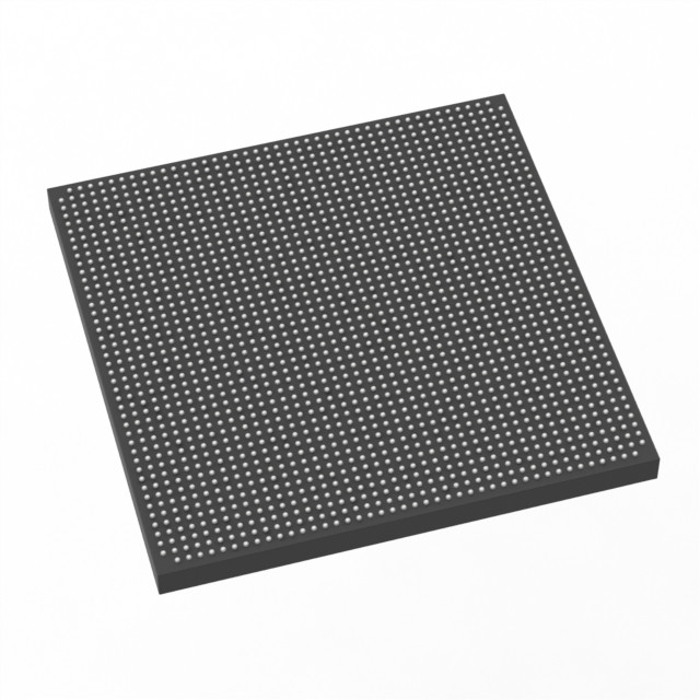
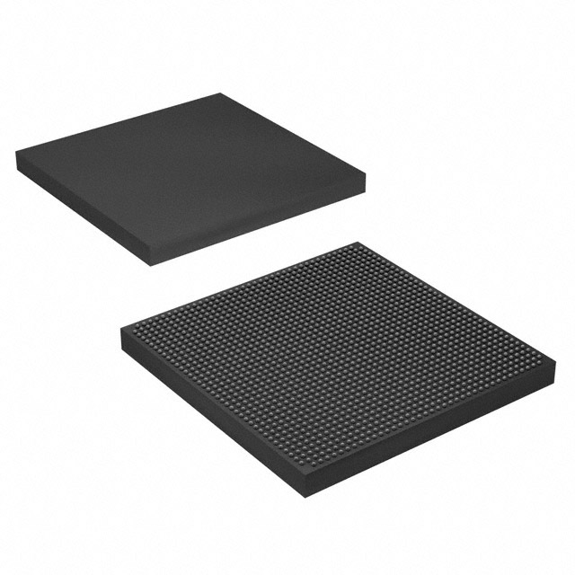
Arria 10 GX Field Programmable Gate Array (FPGA) IC 600 68857856 1150000 1517-BBGA, FCBGA |
|---|---|
| Quantity | 331 Available (as of June 15, 2026) |

| Product Category | Field Programmable Gate Array (FPGA) |
|---|---|
| Manufacturer | Intel |
| Manufacturing Status | Active |
| Manufacturer Standard Lead Time | 16 Weeks |
| Datasheet |
Specifications & Environmental
| Device Package | 1517-FCBGA (40x40) | Grade | Extended | Operating Temperature | 0°C – 100°C | ||
|---|---|---|---|---|---|---|---|
| Package / Case | 1517-BBGA, FCBGA | Number of I/O | 600 | Voltage | 870 mV - 980 mV | ||
| Mounting Method | Surface Mount | RoHS Compliance | RoHS Compliant | REACH Compliance | REACH Unaffected | ||
| Moisture Sensitivity Level | 3 (168 Hours) | Number of LABs/CLBs | 427200 | Number of Logic Elements/Cells | 1150000 | ||
| Number of Gates | N/A | ECCN | 3A001A7A | HTS Code | 8542.39.0001 | ||
| Qualification | N/A | Total RAM Bits | 68857856 |
Overview of 10AX115N2F40E2SG – Arria 10 GX Field Programmable Gate Array (FPGA) IC
The 10AX115N2F40E2SG is an Intel Arria 10 GX-series FPGA device designed for midrange, performance-sensitive applications. Based on the Arria 10 device family architecture, it delivers a high-density, power-conscious programmable fabric optimized for system integration in communications, broadcast, compute and specialized imaging markets.
This device combines a large logic fabric, substantial embedded RAM, and extensive I/O in a 1517-FCBGA package, making it suitable for designs that require dense programmable logic, on-chip memory, and broad external connectivity while operating within defined voltage and temperature windows.
Key Features
- High Logic Density — 1,150,000 logic elements provide substantial programmable capacity for complex digital functions and large-scale logic integration.
- Embedded Memory — 68,857,856 total RAM bits support large on-chip buffering, state storage, and algorithmic working memory.
- Extensive I/O — 600 device I/Os enable wide external interfacing for high-pin-count systems and rich peripheral connectivity.
- Package and Mounting — Supplied in a 1517-FCBGA (1517-BBGA) 40×40 package for surface-mount assembly and compact board-level integration.
- Power Supply Range — Core voltage support from 870 mV to 980 mV, suitable for the device’s specified power architecture.
- Operating Range & Grade — Extended-grade device with an operating temperature range of 0 °C to 100 °C for controlled-environment applications.
- RoHS Compliant — Conforms to RoHS directives for lead-free assembly and environmental compliance.
- Arria 10 Family Attributes — Part of the 20 nm Arria 10 device family described as mid-range FPGAs and SoCs with power-efficiency and higher performance characteristics in its class.
Typical Applications
- Wireless Infrastructure — Channel and switch cards in remote radio heads and mobile backhaul systems where programmable logic and moderate power efficiency are required.
- Wireline Communications — 40G/100G muxponders, transponders, and line cards that benefit from high logic density and abundant I/O for packet processing and data-plane functions.
- Broadcast and Professional AV — Studio switches, transport, and videoconferencing systems requiring flexible, high-capacity logic and on-chip memory for real-time media processing.
- Compute and Storage Acceleration — Flash cache, server acceleration, and cloud compute offloads that leverage large programmable fabrics and embedded RAM for custom acceleration tasks.
- Medical and Defense Electronics — Diagnostic imaging and radar/control subsystems that require scalable logic resources and deterministic hardware implementation.
Unique Advantages
- Substantial Logic Resources: 1,150,000 logic elements enable integration of complex data paths, custom accelerators, and protocol engines on a single device, reducing board-level component count.
- Large On‑Chip Memory: Nearly 69 million RAM bits provide ample on-chip storage for buffering, lookup tables, and intermediate data, improving throughput and latency for memory-intensive algorithms.
- High I/O Count: 600 I/Os support wide external interfacing options for high-density system designs, simplifying routing of multiple peripherals and buses.
- Compact FCBGA Packaging: The 1517-FCBGA (40×40) package delivers a high pin-count footprint in a single, surface-mount module suitable for space-constrained PCBs.
- Arria 10 Family Benefits: Built on the Arria 10 20 nm device family, the device inherits the series focus on performance and power-efficiency for midrange FPGA and SoC applications.
- Environment & Compliance: Extended-grade temperature operation (0 °C to 100 °C) and RoHS compliance support deployment in controlled-environment commercial and industrial designs.
Why Choose 10AX115N2F40E2SG?
The 10AX115N2F40E2SG positions itself as a high-capacity, midrange Arria 10 GX FPGA for designs that need large programmable logic, significant on-chip memory, and wide external connectivity in a compact surface-mount package. Its core voltage window and extended-grade operating temperature make it suitable for controlled-environment communications, broadcast, compute acceleration, and imaging systems.
For engineering teams seeking a programmable platform with measurable logic and memory resources, high I/O density, and the ecosystem association of the Arria 10 family, this device offers a balanced combination of integration and scalability for medium-to-large FPGA designs.
Request a quote or submit your requirements to receive pricing and availability for the 10AX115N2F40E2SG FPGA.


Date Founded: 1968
Headquarters: Santa Clara, California, USA
Employees: 130,000+
Revenue: $54.23 Billion
Certifications and Memberships: ISO9001:2015, ISO14001:2015, ISO17025:2017, ISO27001:2022, ISO45001:2018, ISO50001:2018


