
10AX115N2F40I2SG
| Part Description |
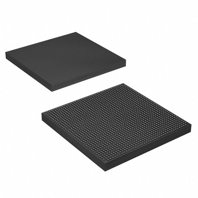
Arria 10 GX Field Programmable Gate Array (FPGA) IC 600 68857856 1150000 1517-BBGA, FCBGA |
|---|---|
| Quantity | 375 Available (as of October 8, 2026) |
| Product Category | Field Programmable Gate Array (FPGA) |
|---|---|
| Manufacturer | Intel |
| Manufacturing Status | Active |
| Manufacturer Standard Lead Time | 16 Weeks |
| Datasheet |
Specifications & Environmental
| Device Package | 1517-FCBGA (40x40) | Grade | Industrial | Operating Temperature | -40°C – 100°C | ||
|---|---|---|---|---|---|---|---|
| Package / Case | 1517-BBGA, FCBGA | Number of I/O | 600 | Voltage | 870 mV - 980 mV | ||
| Mounting Method | Surface Mount | RoHS Compliance | RoHS Compliant | REACH Compliance | REACH Unaffected | ||
| Moisture Sensitivity Level | 3 (168 Hours) | Number of LABs/CLBs | 427200 | Number of Logic Elements/Cells | 1150000 | ||
| Number of Gates | N/A | ECCN | 3A001A7A | HTS Code | 8542.39.0001 | ||
| Qualification | N/A | Total RAM Bits | 68857856 |
Overview of 10AX115N2F40I2SG – Arria 10 GX FPGA, 1,150,000 Logic Elements, 1517-FCBGA
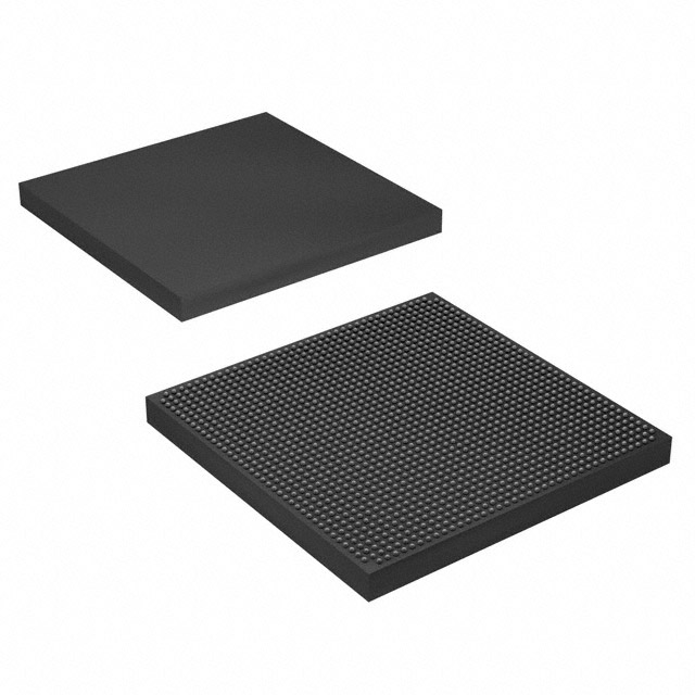
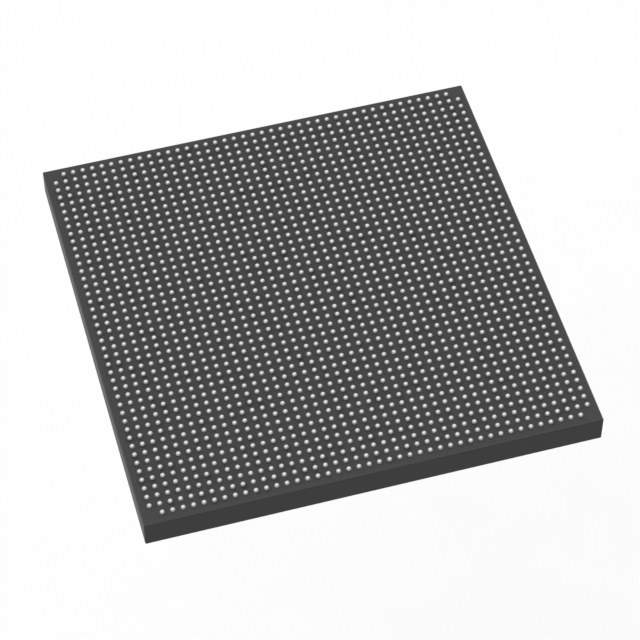
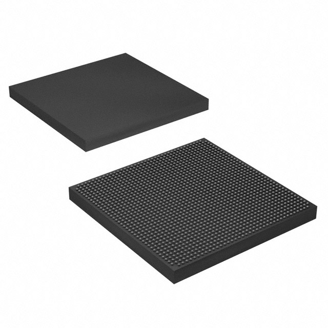
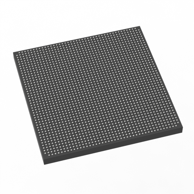
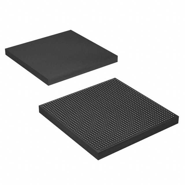
The 10AX115N2F40I2SG is an Intel Arria 10 GX field-programmable gate array (FPGA) in a 1517-FCBGA (40×40) surface-mount package. It is a 20 nm mid-range FPGA offering high logic density, large embedded memory, and broad I/O for compute- and bandwidth‑focused designs.
Designed for markets such as wireless, wireline, broadcast, computing and storage, medical, and military applications, this device targets high-performance, power-sensitive midrange systems that require scalable logic, abundant on-chip RAM, and industrial temperature operation.
Key Features
- Logic Capacity — 1,150,000 logic elements provide high integration for complex processing, control, and protocol implementations.
- Embedded Memory — 68,857,856 total RAM bits enable large on-chip buffers, caches, and packet or frame storage.
- I/O Density — 600 general-purpose I/O pins support extensive external interfacing and parallel connectivity.
- Transceivers & Interfaces — Family-level features include low-power serial transceivers, PCIe Gen1/2/3 hard IP, enhanced PCS hard IP for Interlaken and 10 Gbps Ethernet, and external memory interface support as described in the device overview.
- DSP and Clocking — Variable-precision DSP blocks and comprehensive clock networks with PLL clock sources support precision signal processing and synchronized multi-rate designs.
- Power Supply — Supported core voltage range from 870 mV to 980 mV, enabling controlled power delivery and system-level power planning.
- Package & Mounting — 1517-BBGA / 1517-FCBGA (40×40) surface-mount package for high-density board integration.
- Operating Range & Compliance — Industrial-grade operation from −40 °C to 100 °C and RoHS-compliant material status for regulatory alignment.
Typical Applications
- Wireless Infrastructure — Channel cards, switch cards in remote radio heads, and mobile backhaul systems benefiting from high logic density and low-power transceivers.
- Wireline Networking — 40G/100G muxponders, transponders, and 100G line cards where high-speed interfaces and on-chip buffering are required.
- Broadcast and Media — Studio switches, transport, and videoconferencing equipment leveraging large embedded memory and flexible I/O.
- Compute & Storage Acceleration — Flash cache, cloud server acceleration, and other data-center functions that use abundant logic and RAM for offload tasks.
- Imaging and Defense Systems — Diagnostic imaging, radar, and secure communications that need deterministic operation across an industrial temperature range.
Unique Advantages
- High integration density: 1,150,000 logic elements reduce the need for multi-device solutions and simplify routing and PCB complexity.
- Large on-chip memory: Nearly 69 Mbits of RAM supports substantial buffering, lookup tables, and state storage without external memory for many use cases.
- Broad I/O and protocol support: 600 I/O pins combined with family-level hard IP for PCIe and high‑speed Ethernet support diverse system interfaces.
- Industrial temperature operation: Rated from −40 °C to 100 °C for deployment in temperature-challenging environments.
- Compact, manufacturable package: 1517-FCBGA surface-mount package (40×40) enables compact board-level designs with reliable solder attachment.
- Regulatory alignment: RoHS compliance supports environmental and supply-chain requirements.
Why Choose 10AX115N2F40I2SG?
The 10AX115N2F40I2SG positions itself as a high-density, midrange FPGA solution within the Intel Arria 10 family, delivering a balance of logic capacity, embedded memory, and I/O for demanding system designs. Its 20 nm architecture and family-level support for DSP blocks, transceivers, and hard IP make it suitable for bandwidth- and compute‑oriented applications where power efficiency and integration matter.
This device is well suited for engineering teams building telecommunications, networking, broadcast, compute acceleration, medical imaging, and defense systems that require scalable logic, substantial on-chip RAM, industrial temperature capability, and a compact FCBGA package for system integration.
Request a quote or submit an inquiry to check availability, lead times, and pricing for the 10AX115N2F40I2SG.





















Date Founded: 1968
Headquarters: Santa Clara, California, USA
Employees: 130,000+
Revenue: $54.23 Billion
Certifications and Memberships: ISO9001:2015, ISO14001:2015, ISO17025:2017, ISO27001:2022, ISO45001:2018, ISO50001:2018


