
10AX115U2F45E1SG
| Part Description |
Arria 10 GX Field Programmable Gate Array (FPGA) IC 480 68857856 1150000 1932-BBGA, FCBGA |
|---|---|
| Quantity | 716 Available (as of June 15, 2026) |

| Product Category | Field Programmable Gate Array (FPGA) |
|---|---|
| Manufacturer | Intel |
| Manufacturing Status | Active |
| Manufacturer Standard Lead Time | 16 Weeks |
| Datasheet |
Specifications & Environmental
| Device Package | 1932-FCBGA (45x45) | Grade | Extended | Operating Temperature | 0°C – 100°C | ||
|---|---|---|---|---|---|---|---|
| Package / Case | 1932-BBGA, FCBGA | Number of I/O | 480 | Voltage | 870 mV - 980 mV | ||
| Mounting Method | Surface Mount | RoHS Compliance | RoHS Compliant | REACH Compliance | REACH Unaffected | ||
| Moisture Sensitivity Level | 3 (168 Hours) | Number of LABs/CLBs | 427200 | Number of Logic Elements/Cells | 1150000 | ||
| Number of Gates | N/A | ECCN | 3A001A7A | HTS Code | 8542.39.0001 | ||
| Qualification | N/A | Total RAM Bits | 68857856 |
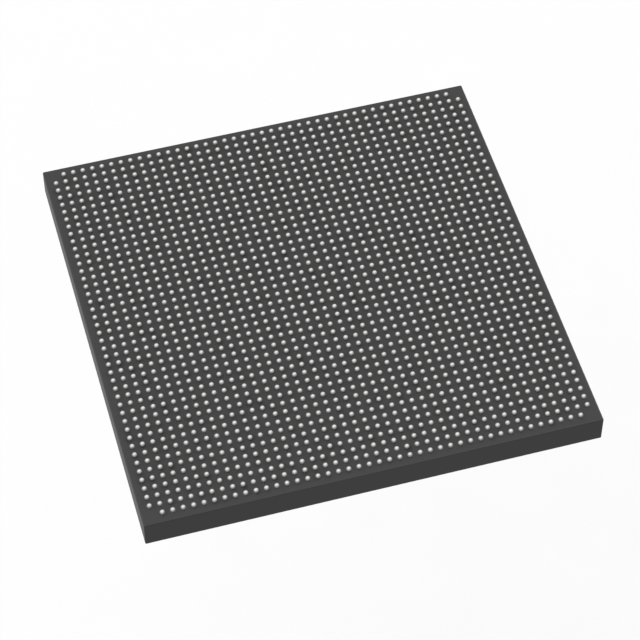
Overview of 10AX115U2F45E1SG – Arria 10 GX FPGA, 1,150,000 logic elements, 1932-FCBGA
The 10AX115U2F45E1SG is an Intel Arria 10 GX Field Programmable Gate Array in a 1932-FCBGA (45×45) package. It is a 20 nm mid-range FPGA family member designed for performance and power-efficient system integration, offering a large programmable fabric alongside substantial embedded memory and I/O resources.
Typical use cases include wireless and wireline infrastructure, broadcast and video transport, compute and storage acceleration, and other mid-range applications that require high logic capacity, abundant RAM, and flexible I/O connectivity.
Key Features
- Logic Capacity 1,150,000 logic elements provide a high-density programmable fabric for complex digital designs and large-scale integration.
- Embedded Memory 68,857,856 total RAM bits support deep buffering, on-chip data storage, and memory-intensive processing without relying solely on external memory.
- I/O Resources 480 available I/O pins in the device enable broad peripheral connectivity and multi-channel interface implementations.
- Package & Mounting Supplied in a 1932-BBGA/1932-FCBGA (45×45) package optimized for surface-mount PCB assembly and high I/O density.
- Voltage & Power Core supply range of 870 mV to 980 mV to match system power budgeting and regulator choices.
- Operating Range Extended grade device with an operating temperature range of 0 °C to 100 °C for deployment in standard industrial and commercial environments.
- Series Capabilities (Arria 10) Series-level features include 20 nm architecture, embedded DSP blocks, PLL clock management, transceiver and Ethernet/PCIe hard-IP options, and support for dynamic/partial reconfiguration as documented in the Arria 10 device overview.
- Compliance RoHS compliant for environmental and regulatory alignment in modern electronics manufacturing.
Typical Applications
- Wireless Infrastructure Channel and switch cards in remote radio heads and mobile backhaul systems that need programmable logic and on-chip memory for signal processing.
- Wireline Communications 40G/100G muxponders, transponders, and 100G line cards where high logic density and robust I/O support complex protocol and packet-processing stacks.
- Broadcast & Video Transport Studio switching, professional audio/video processing, and transport applications using large on-chip buffers and flexible interfacing.
- Compute & Storage Acceleration Server-side acceleration and flash-cache applications that leverage programmable logic and embedded RAM for custom data-path and caching functions.
- Medical Imaging & Diagnostics Diagnostic scanners and imaging systems requiring sizable on-chip memory and logic for real-time data aggregation and preprocessing.
Unique Advantages
- High Logic Density: 1,150,000 logic elements let you implement large custom datapaths and complex control logic on a single device, reducing component count.
- Substantial On‑Chip Memory: Nearly 69 million RAM bits enable deep buffering and on-FPGA data handling for lower external memory dependency and reduced latency.
- Rich I/O Count and Packaging: 480 I/Os in a 1932-FCBGA (45×45) package provide the pin density and form factor needed for multi-channel systems and compact PCB designs.
- Series-Level Signal Processing & Interfaces: Arria 10 family features documented in the device overview—DSP blocks, clock/PLL networks, transceivers, and protocol hard IP—support complex communications and signal-processing functions.
- Design and Documentation Support: The device is part of the Intel Arria 10 family and is supported by Intel’s device documentation and handbooks for design guidance and errata references.
- Regulatory Readiness: RoHS compliance simplifies environmental conformity during product manufacturing.
Why Choose 10AX115U2F45E1SG?
The 10AX115U2F45E1SG positions itself as a high-capacity, mid-range FPGA option within the Arria 10 GX family, combining large logic and memory resources with extensive I/O and a compact 1932-FCBGA package. Its documented series capabilities—20 nm architecture, DSP resources, PLLs, transceiver and protocol hard IP, and support for dynamic configuration—make it suitable for designs requiring significant on-chip processing, buffering, and flexible interfacing.
Engineers and procurement teams targeting wireless/wireline infrastructure, broadcast systems, compute acceleration, or imaging applications will find the device’s balance of integration, documentation, and environmental compliance useful for scalable product development and long-term platform support.
Request a quote or submit an inquiry to get pricing and availability for the 10AX115U2F45E1SG.


Date Founded: 1968
Headquarters: Santa Clara, California, USA
Employees: 130,000+
Revenue: $54.23 Billion
Certifications and Memberships: ISO9001:2015, ISO14001:2015, ISO17025:2017, ISO27001:2022, ISO45001:2018, ISO50001:2018


