
5AGXFA5H4F35C4N
| Part Description |
Arria V GX Field Programmable Gate Array (FPGA) IC 544 13284352 190000 1152-BBGA, FCBGA Exposed Pad |
|---|---|
| Quantity | 1,184 Available (as of June 15, 2026) |

| Product Category | Field Programmable Gate Array (FPGA) |
|---|---|
| Manufacturer | Intel |
| Manufacturing Status | Obsolete |
| Manufacturer Standard Lead Time | Contact Us |
| Datasheet |
Specifications & Environmental
| Device Package | 1152-FBGA (35x35) | Grade | Commercial | Operating Temperature | 0°C – 85°C | ||
|---|---|---|---|---|---|---|---|
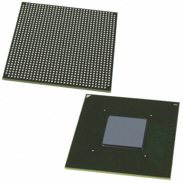
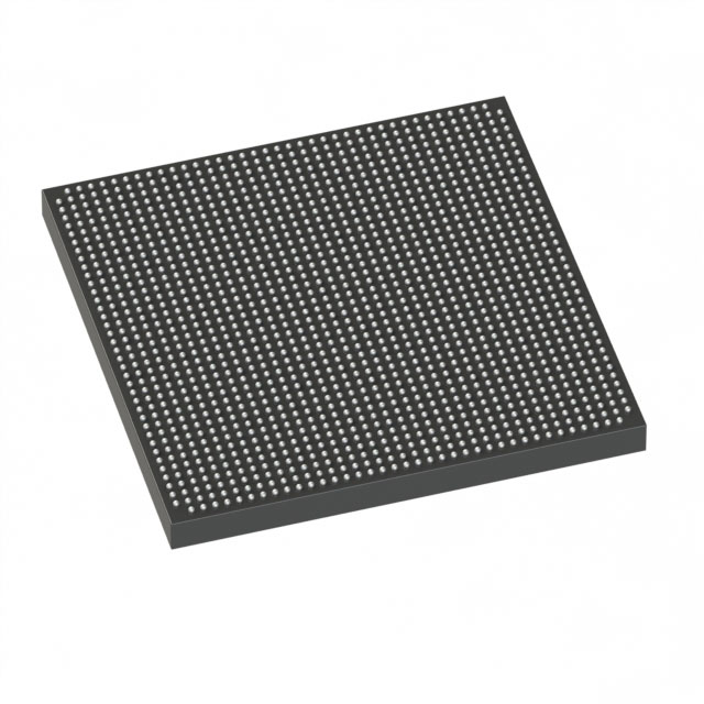
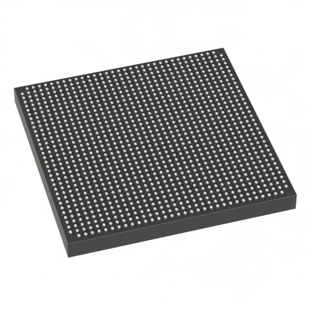
| Package / Case | 1152-BBGA, FCBGA Exposed Pad | Number of I/O | 544 | Voltage | 1.07 V - 1.13 V | ||
| Mounting Method | Surface Mount | RoHS Compliance | RoHS Compliant | REACH Compliance | REACH Unknown | ||
| Moisture Sensitivity Level | 3 (168 Hours) | Number of LABs/CLBs | 8962 | Number of Logic Elements/Cells | 190000 | ||
| Number of Gates | N/A | ECCN | 3A001A2C | HTS Code | 8542.39.0001 | ||
| Qualification | N/A | Total RAM Bits | 13284352 |
Overview of 5AGXFA5H4F35C4N – Arria V GX FPGA, 1152-FBGA (35×35)
The 5AGXFA5H4F35C4N is an Arria V GX Field Programmable Gate Array (FPGA) IC from Intel, supplied in a 1152-ball FCBGA exposed pad package. It delivers a high-density programmable logic fabric combined with substantial embedded memory and a large I/O count for complex digital designs.
With 190,000 logic elements, approximately 12.7 Mbits of embedded RAM, and 544 I/O, this commercial‑grade FPGA is suited to designs that require significant logic capacity, on‑chip buffering, and broad external connectivity while operating within standard commercial temperature and supply voltage ranges.
Key Features
- Core Logic: 190,000 logic elements provide substantial programmable fabric for implementing complex custom logic, state machines, and parallel datapaths.
- Embedded Memory: Approximately 12.7 Mbits of on‑chip RAM for frame buffers, lookup tables, and local data storage to support high‑throughput processing and low‑latency pipelines.
- I/O Density: 544 available I/O pins to enable comprehensive interfacing with peripherals, high‑speed transceivers, and multi‑lane buses.
- Power Supply Range: Operates from a core supply of 1.07 V to 1.13 V, enabling predictable power budgeting in system designs.
- Package & Mounting: 1152-BBGA (1152-FBGA, 35×35) with exposed pad and surface mount construction for compact board integration.
- Operating Conditions: Commercial temperature rating from 0 °C to 85 °C, suitable for standard commercial applications.
- Environmental Compliance: RoHS compliant to support regulatory requirements for lead‑free assembly.
Typical Applications
- Networking & Data Communications: High I/O count and substantial logic elements support packet processing, protocol bridging, and custom interface implementations.
- Signal Processing & Acceleration: Large embedded RAM and dense logic fabric enable implementation of DSP pipelines, FIR/IIR filters, and acceleration blocks for compute‑intensive tasks.
- Custom Compute & Control: Programmable logic and generous I/O allow tailored control systems, hardware accelerators, and glue logic for complex electronics.
- Prototyping & Development: Offers the capacity to prototype large FPGA designs that require scalable logic, memory, and I/O resources within a commercial product envelope.
Unique Advantages
- High Logic Capacity: 190,000 logic elements provide headroom for large, parallelized designs and complex state machines without immediate redesign.
- Substantial On‑Chip Memory: Approximately 12.7 Mbits of embedded RAM reduces external memory dependencies and improves data locality for lower latency.
- Extensive I/O Connectivity: 544 I/O pins enable flexible interfacing options and simplify integration with multi‑lane or multi‑device systems.
- Compact Package Integration: 1152‑ball FCBGA exposed pad package supports dense board layouts and thermal conduction through the exposed pad.
- Commercial Temperature Suitability: Rated 0 °C to 85 °C for deployments in standard commercial environments where controlled ambient conditions are expected.
- RoHS Compliance: Conforms to RoHS requirements for lead‑free manufacturing and regulatory compatibility.
Why Choose 5AGXFA5H4F35C4N?
The 5AGXFA5H4F35C4N Arria V GX FPGA balances high logic density, meaningful on‑chip RAM, and a large I/O footprint in a compact FCBGA package, making it a solid choice for commercial designs that require integrated programmable logic and substantial interfacing. Its defined supply and temperature ranges allow predictable system-level integration and power planning.
This device is well suited to engineering teams building high‑throughput digital designs, protocol adapters, and custom accelerators that benefit from on‑chip memory and extensive I/O. The combination of capacity and package density supports scalable designs that can be adapted as requirements evolve.
Request a quote or submit an inquiry to receive pricing and availability details for the 5AGXFA5H4F35C4N Arria V GX FPGA.


Date Founded: 1968
Headquarters: Santa Clara, California, USA
Employees: 130,000+
Revenue: $54.23 Billion
Certifications and Memberships: ISO9001:2015, ISO14001:2015, ISO17025:2017, ISO27001:2022, ISO45001:2018, ISO50001:2018


