
5AGXFB7K4F40C4G
| Part Description |
Arria V GX Field Programmable Gate Array (FPGA) IC 704 2975744 504140 1517-BBGA, FCBGA |
|---|---|
| Quantity | 1,039 Available (as of June 14, 2026) |

| Product Category | Field Programmable Gate Array (FPGA) |
|---|---|
| Manufacturer | Intel |
| Manufacturing Status | Active |
| Manufacturer Standard Lead Time | 16 Weeks |
| Datasheet |
Specifications & Environmental
| Device Package | 1517-FBGA, FC (40x40) | Grade | Commercial | Operating Temperature | 0°C – 85°C | ||
|---|---|---|---|---|---|---|---|
| Package / Case | 1517-BBGA, FCBGA | Number of I/O | 704 | Voltage | 1.07 V - 1.13 V | ||
| Mounting Method | Surface Mount | RoHS Compliance | RoHS Compliant | REACH Compliance | REACH Unaffected | ||
| Moisture Sensitivity Level | 3 (168 Hours) | Number of LABs/CLBs | 23786 | Number of Logic Elements/Cells | 504140 | ||
| Number of Gates | N/A | ECCN | N/A | HTS Code | N/A | ||
| Qualification | N/A | Total RAM Bits | 2975744 |
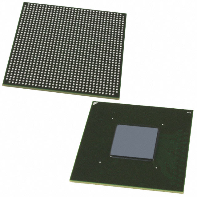
Overview of 5AGXFB7K4F40C4G – Arria V GX FPGA, 504,140 logic elements, 704 I/Os
The 5AGXFB7K4F40C4G is an Intel Arria V GX Field Programmable Gate Array (FPGA) in a 1517-BBGA FCBGA package, offered in a commercial grade. It provides a large pool of programmable logic, substantial on-chip RAM, and high I/O density for designs that require significant integration of digital functions.
Delivered as a surface-mount 1517-FBGA (40×40) device, this FPGA is specified with a core supply range of 1.07 V to 1.13 V and an operating temperature range of 0 °C to 85 °C. The available datasheet provides detailed electrical characteristics, switching and configuration specifications, and I/O timing guidance for system integration.
Key Features
- Large programmable logic capacity — 504,140 logic elements and 23,786 CLBs provide extensive resources for combining custom logic, glue logic, and processing engines on a single device.
- Embedded memory — approximately 2.98 Mbits of on-chip RAM for buffering, state storage, and local data structures.
- High I/O count — 704 I/O pins to support dense external interfaces and multiple parallel buses.
- Power supply — defined core voltage operating range of 1.07 V to 1.13 V to match targeted power delivery designs.
- Commercial grade and thermal range — specified for 0 °C to 85 °C operation, suitable for standard commercial electronic environments.
- Package and mounting — 1517-BBGA, FCBGA package (supplier package: 1517-FBGA, FC, 40×40); surface-mount for PCB assembly.
- Standards and compliance — RoHS-compliant for environmental and assembly requirements.
- Comprehensive documentation — datasheet coverage includes electrical characteristics, switching characteristics, configuration specifications, and I/O timing for integration and validation.
Typical Applications
- High-density programmable systems — designs that require hundreds of thousands of logic elements and flexible on-chip logic partitioning.
- Memory-intensive functions — applications that leverage approximately 2.98 Mbits of embedded RAM for buffering, FIFOs, and small local data stores.
- I/O-dense interfaces — platforms requiring up to 704 I/Os for parallel buses, multi-channel I/O, or complex interface bridging.
- Commercial electronic products — systems operating within a 0 °C to 85 °C range seeking a commercial-grade FPGA solution.
Unique Advantages
- Substantial logic resources: 504,140 logic elements enable consolidation of multiple functions into a single device, reducing board-level complexity.
- Significant on-chip memory: approximately 2.98 Mbits of RAM supports local data handling and reduces external memory dependencies.
- High I/O bandwidth: 704 I/Os provide flexibility for multi-channel connectivity and dense peripheral integration.
- Compact FCBGA package: 1517-BBGA (1517-FBGA, 40×40) footprint supports high-density PCB layouts while maintaining surface-mount assembly compatibility.
- Defined power envelope: narrow core supply range (1.07 V–1.13 V) aids in power-supply design and stability for the FPGA core.
- Documented integration guidance: the datasheet supplies the electrical, switching, and configuration specifications needed for reliable system integration.
Why Choose 5AGXFB7K4F40C4G?
The 5AGXFB7K4F40C4G Arria V GX FPGA combines a large logic fabric, measurable on-chip memory, and a high pin count in a commercial-grade FCBGA package. Its defined electrical and thermal specifications make it a practical choice for designers consolidating multiple digital functions into a single programmable device.
Backed by comprehensive datasheet documentation covering electrical characteristics, switching behavior, configuration, and I/O timing, this Intel-manufactured FPGA is positioned for projects that need detailed integration guidance, scalability in logic and memory resources, and RoHS-compliant assembly.
Request a quote or submit an inquiry to learn about current availability and pricing for the 5AGXFB7K4F40C4G Arria V GX FPGA.


Date Founded: 1968
Headquarters: Santa Clara, California, USA
Employees: 130,000+
Revenue: $54.23 Billion
Certifications and Memberships: ISO9001:2015, ISO14001:2015, ISO17025:2017, ISO27001:2022, ISO45001:2018, ISO50001:2018


