
5AGXFB7H4F35I5G
| Part Description |
Arria V GX Field Programmable Gate Array (FPGA) IC 544 27695104 504000 1152-BBGA, FCBGA |
|---|---|
| Quantity | 836 Available (as of June 9, 2026) |
| Product Category | Field Programmable Gate Array (FPGA) |
|---|---|
| Manufacturer | Intel |
| Manufacturing Status | Active |
| Manufacturer Standard Lead Time | 16 Weeks |
| Datasheet |
Specifications & Environmental
| Device Package | 1152-FBGA, FC (35x35) | Grade | Industrial | Operating Temperature | -40°C – 100°C | ||
|---|---|---|---|---|---|---|---|
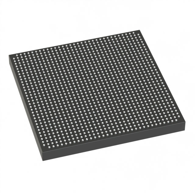
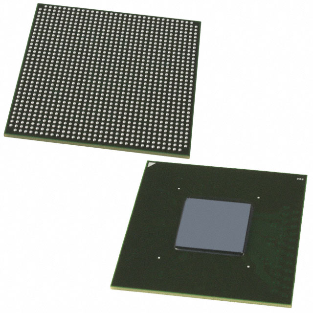
| Package / Case | 1152-BBGA, FCBGA | Number of I/O | 544 | Voltage | 1.07 V - 1.13 V | ||
| Mounting Method | Surface Mount | RoHS Compliance | Unknown | REACH Compliance | REACH Unaffected | ||
| Moisture Sensitivity Level | 3 (168 Hours) | Number of LABs/CLBs | 23780 | Number of Logic Elements/Cells | 504000 | ||
| Number of Gates | N/A | ECCN | 3A001A2C | HTS Code | 8542.39.0001 | ||
| Qualification | N/A | Total RAM Bits | 27695104 |
Overview of 5AGXFB7H4F35I5G – Arria V GX FPGA, 504,000 logic elements, 544 I/O, 1152-BBGA
The 5AGXFB7H4F35I5G is an Intel Arria V GX field programmable gate array (FPGA) offering high logic capacity, abundant I/O, and substantial on-chip memory for complex, programmable digital designs. Its combination of 504,000 logic elements, approximately 27.7 Mbits of embedded memory, and 544 I/O pins makes it suitable for designs that require dense logic integration and flexible interfacing.
Key Features
- Core Logic 504,000 logic elements provide a large programmable fabric for implementing complex digital functions and custom logic blocks.
- Embedded Memory Approximately 27.7 Mbits of on-chip RAM deliver significant storage for buffering, FIFOs, and memory-intensive processing within the FPGA.
- I/O Density 544 programmable I/O pins enable extensive external connectivity for high-pin-count system interfaces and peripherals.
- Power Supply Operates from a specified core voltage range of 1.07 V to 1.13 V for the device core supply requirements.
- Package and Mounting Supplied in a 1152-BBGA, FCBGA package (supplier device package: 1152-FBGA, FC (35x35)) and designed for surface-mount assembly.
- Industrial Temperature Range Rated for operation from -40 °C to 100 °C, suitable for industrial environments requiring extended temperature tolerance.
- RoHS Compliant Meets RoHS environmental requirements as indicated by its compliance status.
Typical Applications
- High-density digital processing — Implement complex custom logic, parallel processing, and protocol engines using the large logic resource pool.
- Memory-intensive designs — Use the on-chip RAM for buffering, packet processing, and storage of intermediate data in embedded systems.
- High-pin-count interfacing — Leverage 544 I/O pins to connect to multiple peripherals, high-speed transceivers, or multi-lane interfaces in system designs.
- Industrial systems — Deploy in applications that require extended temperature operation and robust surface-mount packaging.
Unique Advantages
- Large programmable fabric: 504,000 logic elements enable implementation of extensive custom logic without external ASICs or additional FPGAs.
- Substantial on-chip memory: Approximately 27.7 Mbits of embedded RAM reduces dependence on external memory for many buffering and storage tasks.
- Extensive I/O capability: 544 I/O pins simplify system integration by supporting multiple interfaces and parallel connections directly to the FPGA.
- Industrial-grade temperature range: -40 °C to 100 °C rating supports deployment in temperature-challenging environments.
- Compact FCBGA package: 1152-ball BGA packaging in the supplier-specified 1152-FBGA, FC (35x35) format enables high-density PCB designs with reliable surface-mount assembly.
- Tight core supply specification: The defined 1.07 V to 1.13 V core voltage range supports predictable power design and supply rail planning.
Why Choose 5AGXFB7H4F35I5G?
The 5AGXFB7H4F35I5G positions itself as a high-capacity, industrial-grade FPGA suited for dense logic implementations and memory-rich designs. Its combination of 504,000 logic elements, roughly 27.7 Mbits of on-chip RAM, and 544 I/O pins provides a balanced platform for integrating complex processing, buffering, and extensive external interfacing within a single device.
Engineers and procurement teams seeking scalability, robust temperature performance, and a compact BGA package will find this FPGA advantageous for mid-to-high complexity systems where integration and I/O count are critical. The device’s clear electrical and package specifications support predictable integration into tight board-level designs.
Request a quote or submit an inquiry to receive pricing and availability information for 5AGXFB7H4F35I5G and to discuss how it fits your project requirements.


Date Founded: 1968
Headquarters: Santa Clara, California, USA
Employees: 130,000+
Revenue: $54.23 Billion
Certifications and Memberships: ISO9001:2015, ISO14001:2015, ISO17025:2017, ISO27001:2022, ISO45001:2018, ISO50001:2018


