
5AGXMB1G6F31C6G
| Part Description |
Arria V GX Field Programmable Gate Array (FPGA) IC 384 17358848 300000 896-BBGA, FCBGA |
|---|---|
| Quantity | 1,695 Available (as of June 15, 2026) |
| Product Category | Field Programmable Gate Array (FPGA) |
|---|---|
| Manufacturer | Intel |
| Manufacturing Status | Active |
| Manufacturer Standard Lead Time | 12 Weeks |
| Datasheet |
Specifications & Environmental
| Device Package | 896-FBGA (31x31) | Grade | Commercial | Operating Temperature | 0°C – 85°C | ||
|---|---|---|---|---|---|---|---|
| Package / Case | 896-BBGA, FCBGA | Number of I/O | 384 | Voltage | 1.07 V - 1.13 V | ||
| Mounting Method | Surface Mount | RoHS Compliance | RoHS Compliant | REACH Compliance | REACH Unaffected | ||
| Moisture Sensitivity Level | 3 (168 Hours) | Number of LABs/CLBs | 14151 | Number of Logic Elements/Cells | 300000 | ||
| Number of Gates | N/A | ECCN | PENDING ECCN | HTS Code | 0000.00.0000 | ||
| Qualification | N/A | Total RAM Bits | 17358848 |
Overview of 5AGXMB1G6F31C6G – Arria V GX FPGA, 300,000 logic elements, 384 I/O, 896-BBGA
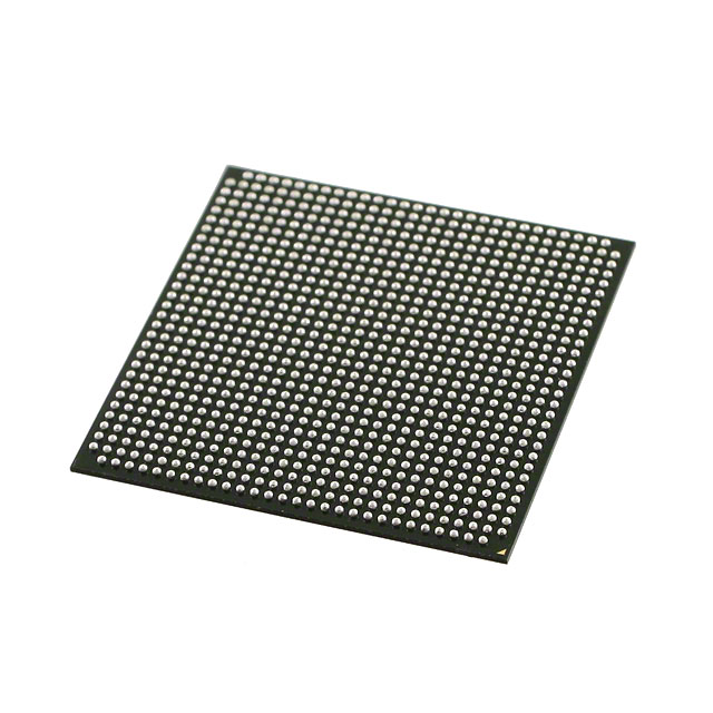
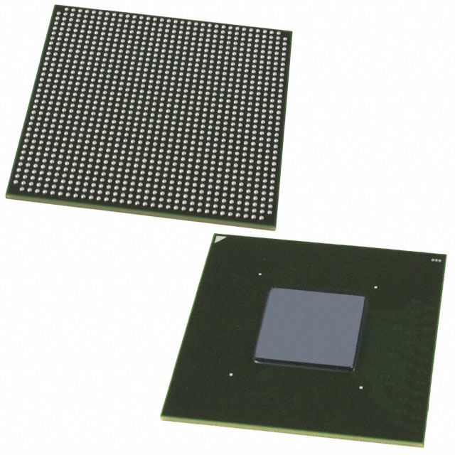
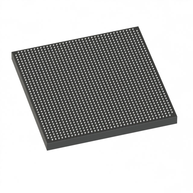
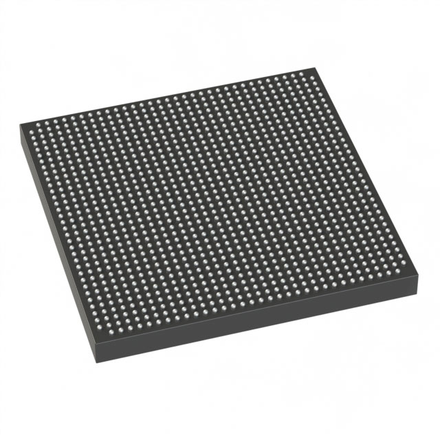
The 5AGXMB1G6F31C6G is an Arria V GX field-programmable gate array (FPGA) in a surface-mount 896-ball BGA package. This commercial‑grade device integrates 300,000 logic elements and approximately 17.36 Mbits of embedded RAM to support complex, high‑density digital designs.
With 384 user I/O, a tightly controlled core supply range (1.07 V to 1.13 V), and an operating temperature range of 0 °C to 85 °C, the device targets applications that require significant on‑chip logic, abundant memory, and extensive I/O connectivity in a compact FCBGA footprint.
Key Features
- Logic Capacity 300,000 logic elements to implement large combinational and sequential logic functions.
- Embedded Memory Approximately 17.36 Mbits of on‑chip RAM for buffering, FIFOs, and memory‑mapped logic structures.
- High I/O Count 384 user I/O pins to support wide parallel interfaces and diverse peripheral connectivity.
- Package & Mounting 896‑ball FCBGA (896‑BBGA, 31×31) package designed for surface‑mount assembly and dense board integration.
- Power Core supply voltage specified between 1.07 V and 1.13 V for defined core operation.
- Operating Range Commercial grade device rated for 0 °C to 85 °C ambient operating temperature.
- Compliance RoHS compliant.
Typical Applications
- High‑Density Digital Systems Large logic capacity and embedded RAM make the device suitable for complex pattern processing and protocol implementation.
- Multi‑I/O Interface Hubs 384 I/O pins enable aggregation and bridging between multiple parallel or parallel/serial interfaces.
- Embedded Acceleration On‑chip memory and abundant logic elements support hardware acceleration and custom datapath designs.
Unique Advantages
- Substantial Logic Resources: 300,000 logic elements provide the headroom to integrate large custom logic blocks and control functions on a single device.
- Significant Embedded RAM: Approximately 17.36 Mbits of on‑chip memory reduces external memory dependency for buffering and state storage.
- High I/O Density: 384 user I/O simplifies board routing and minimizes the need for multiple interface chips.
- Compact BGA Package: 896‑ball FCBGA (31×31) delivers high pin count in a compact footprint for space‑constrained designs.
- Deterministic Core Power Range: Clearly defined core voltage (1.07 V–1.13 V) supports precise power planning and thermal design.
- Commercial Grade Availability: Designed for commercial temperature environments (0 °C–85 °C) for mainstream embedded and communications products.
Why Choose 5AGXMB1G6F31C6G?
The 5AGXMB1G6F31C6G Arria V GX FPGA combines substantial logic density, embedded memory, and a high I/O count in a compact 896‑ball FCBGA package, offering a balanced platform for demanding digital designs. Its defined core supply range and commercial operating temperature make it suitable for systems where integration, deterministic power planning, and dense I/O are priorities.
This device is well suited to engineering teams designing mid‑ to high‑complexity FPGA solutions that require on‑chip memory, extensive interfacing, and a compact board footprint, while maintaining RoHS compliance and commercial temperature support.
Request a quote or submit an inquiry to receive pricing and availability information for 5AGXMB1G6F31C6G.


Date Founded: 1968
Headquarters: Santa Clara, California, USA
Employees: 130,000+
Revenue: $54.23 Billion
Certifications and Memberships: ISO9001:2015, ISO14001:2015, ISO17025:2017, ISO27001:2022, ISO45001:2018, ISO50001:2018


