
5AGXMB5G4F35C4N
| Part Description |
Arria V GX Field Programmable Gate Array (FPGA) IC 544 23625728 420000 1152-BBGA, FCBGA Exposed Pad |
|---|---|
| Quantity | 1,053 Available (as of June 15, 2026) |

| Product Category | Field Programmable Gate Array (FPGA) |
|---|---|
| Manufacturer | Intel |
| Manufacturing Status | Obsolete |
| Manufacturer Standard Lead Time | Contact Us |
| Datasheet |
Specifications & Environmental
| Device Package | 1152-FBGA (35x35) | Grade | Commercial | Operating Temperature | 0°C – 85°C | ||
|---|---|---|---|---|---|---|---|
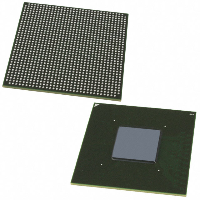
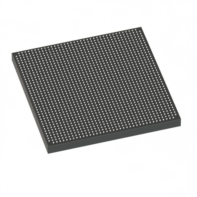
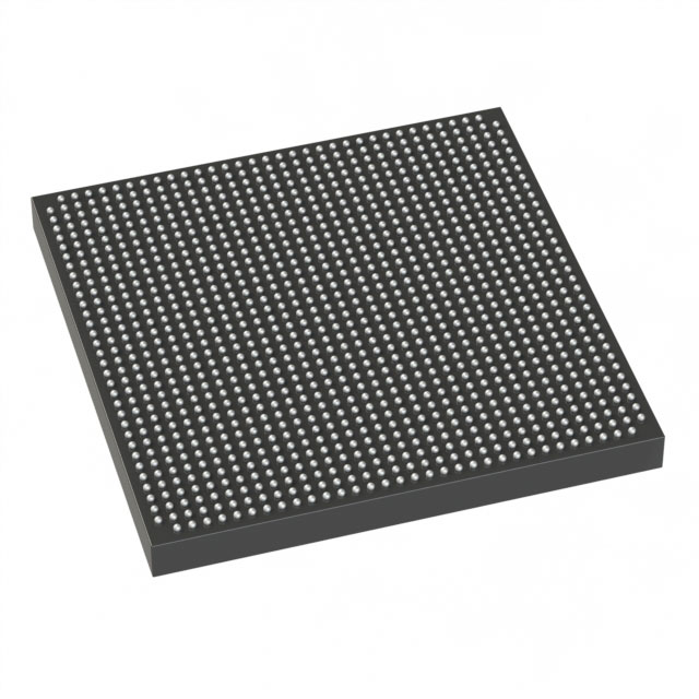
| Package / Case | 1152-BBGA, FCBGA Exposed Pad | Number of I/O | 544 | Voltage | 1.07 V - 1.13 V | ||
| Mounting Method | Surface Mount | RoHS Compliance | RoHS Compliant | REACH Compliance | REACH Unknown | ||
| Moisture Sensitivity Level | 3 (168 Hours) | Number of LABs/CLBs | 19811 | Number of Logic Elements/Cells | 420000 | ||
| Number of Gates | N/A | ECCN | 3A001A2C | HTS Code | 8542.39.0001 | ||
| Qualification | N/A | Total RAM Bits | 23625728 |
Overview of 5AGXMB5G4F35C4N – Arria V GX Field Programmable Gate Array (FPGA)
The 5AGXMB5G4F35C4N is an Arria V GX family FPGA in a 1152-ball BGA exposed-pad package, offered in a commercial grade and designed for surface-mount assembly. It provides high logic density, substantial embedded memory, and a large I/O count for designs that require significant programmable logic and connectivity.
Key technical attributes include 420,000 logic elements, approximately 23.6 Mbits of on-chip RAM, and up to 544 I/O pins, combined with a tightly specified core voltage range (1.07 V to 1.13 V) and an ambient operating range of 0 °C to 85 °C.
Key Features
- Core Logic — 420,000 logic elements to implement large-scale custom logic, control functions, and datapath resources.
- Embedded Memory — Approximately 23.6 Mbits of on-chip RAM (23,625,728 bits) for buffering, FIFOs, and on-chip data storage.
- I/O Capacity — Up to 544 available I/O pins, enabling broad external device interfacing and high-channel connectivity.
- Package — 1152-BBGA, FCBGA exposed pad package; supplier device package listed as 1152-FBGA (35×35), optimized for high-density board designs and thermal management through the exposed pad.
- Power Supply — Narrow core voltage operating window: 1.07 V to 1.13 V, enabling consistent core performance when designed to the specified rail.
- Operating Temperature — Commercial grade operation from 0 °C to 85 °C for standard commercial applications.
- Mounting & Compliance — Surface mount device with RoHS compliance for environmental and manufacturing requirements.
Typical Applications
- High-density programmable logic — Implement complex digital functions and custom hardware accelerators where up to 420,000 logic elements are required.
- Large I/O systems — Systems requiring extensive external interfacing or parallel connectivity can utilize the device’s 544 I/O pins.
- On-chip buffering and data handling — Designs that need substantial embedded RAM for packet buffering, frame storage, or intermediate data staging benefit from approximately 23.6 Mbits of RAM.
Unique Advantages
- High logic density: 420,000 logic elements give designers the capacity to implement complex, large-scale designs without immediate up-scaling.
- Significant embedded memory: Approximately 23.6 Mbits of on-chip RAM reduces reliance on external memory for many buffering and temporary storage tasks.
- Extensive I/O: 544 available I/Os simplify integration with multiple peripherals, sensors, and parallel interfaces.
- Compact, thermally aware package: 1152-BBGA with exposed pad (1152-FBGA, 35×35) supports high-density PCB layouts and provides a path for thermal dissipation through the exposed pad.
- Controlled supply requirements: A narrow core voltage range (1.07 V–1.13 V) enables predictable power-rail design and voltage budgeting.
- RoHS compliant: Supports environmentally conscious manufacturing and assembly processes.
Why Choose 5AGXMB5G4F35C4N?
The 5AGXMB5G4F35C4N Arria V GX FPGA combines substantial logic capacity, generous embedded memory, and a high I/O count in a commercial-grade, surface-mount package. These characteristics make it well-suited to projects that need on-chip resources to minimize external components while maintaining design flexibility.
This device is appropriate for engineering teams and procurement seeking a high-density programmable solution with clear electrical and thermal packaging attributes, predictable supply requirements, and RoHS compliance for standard commercial deployments.
Request a quote or submit an inquiry to obtain pricing, availability, and lead-time information for the 5AGXMB5G4F35C4N Arria V GX FPGA.


Date Founded: 1968
Headquarters: Santa Clara, California, USA
Employees: 130,000+
Revenue: $54.23 Billion
Certifications and Memberships: ISO9001:2015, ISO14001:2015, ISO17025:2017, ISO27001:2022, ISO45001:2018, ISO50001:2018


