
5AGXMB3G6F35C6N
| Part Description |
Arria V GX Field Programmable Gate Array (FPGA) IC 544 19822592 362000 1152-BBGA, FCBGA Exposed Pad |
|---|---|
| Quantity | 574 Available (as of June 15, 2026) |
| Product Category | Field Programmable Gate Array (FPGA) |
|---|---|
| Manufacturer | Intel |
| Manufacturing Status | Obsolete |
| Manufacturer Standard Lead Time | Contact Us |
| Datasheet |
Specifications & Environmental
| Device Package | 1152-FBGA (35x35) | Grade | Commercial | Operating Temperature | 0°C – 85°C | ||
|---|---|---|---|---|---|---|---|
| Package / Case | 1152-BBGA, FCBGA Exposed Pad | Number of I/O | 544 | Voltage | 1.07 V - 1.13 V | ||
| Mounting Method | Surface Mount | RoHS Compliance | RoHS Compliant | REACH Compliance | REACH Unknown | ||
| Moisture Sensitivity Level | 3 (168 Hours) | Number of LABs/CLBs | 17110 | Number of Logic Elements/Cells | 362000 | ||
| Number of Gates | N/A | ECCN | 3A001A2C | HTS Code | 8542.39.0001 | ||
| Qualification | N/A | Total RAM Bits | 19822592 |
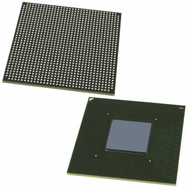
Overview of 5AGXMB3G6F35C6N – Arria V GX FPGA (544 I/O, 362,000 logic elements, 1152-BBGA)
The 5AGXMB3G6F35C6N is an Arria V GX family Field Programmable Gate Array (FPGA) from Intel, offered as a commercial-grade device. It provides a high-density programmable fabric with 362,000 logic elements, approximately 19.8 Mbits of embedded RAM, and 544 user I/O for designs requiring substantial on-chip logic, memory and I/O resources.
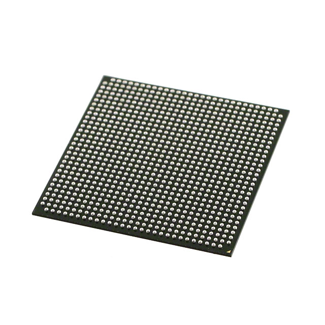
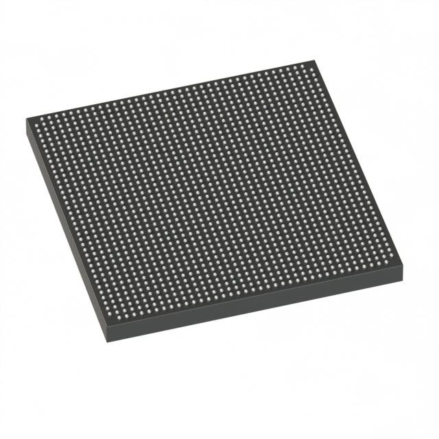
Packaged in a 1152-BBGA (1152-FBGA, 35×35) with exposed pad and intended for surface-mount assembly, this device targets applications that need dense integration and flexible I/O in a commercially rated temperature range.
Key Features
- Core Density 362,000 logic elements to implement substantial digital logic and complex state machines.
- Embedded Memory Approximately 19.8 Mbits of on-chip RAM for buffering, lookup tables, and local data storage.
- I/O Capability 544 dedicated I/O pins to support high channel counts, parallel interfaces, and complex board-level connectivity.
- Power Supply Specified supply range of 1.07 V to 1.13 V, providing defined operating conditions for the core.
- Package & Mounting 1152-BBGA package (supplier device package: 1152-FBGA, 35×35) with exposed pad; designed for surface-mount PCB assembly.
- Commercial Temperature Grade Rated for 0 °C to 85 °C operation to suit standard commercial-environment applications.
- Regulatory RoHS compliant.
Typical Applications
- High-density digital processing Leverage the 362,000 logic elements and substantial embedded RAM for complex logic pipelines and data-path implementations.
- Multi-channel I/O aggregation Use the 544 I/O pins to consolidate multiple interfaces or high-pin-count peripheral connections on a single device.
- Interface bridging and protocol conversion Embedded logic and memory enable implementation of protocol conversion, buffering, and timing adaptation within commercial systems.
Unique Advantages
- High integration density: 362,000 logic elements and approximately 19.8 Mbits of embedded RAM reduce the need for external components and simplify board-level design.
- Extensive I/O resources: 544 I/O pins provide flexibility for complex interconnects and high-channel-count designs without multiple interface chips.
- Defined power envelope: Narrow core supply range (1.07 V–1.13 V) simplifies power-supply design and validation.
- Commercial grade: Rated for 0 °C to 85 °C operation to match standard commercial product environments.
- Surface-mount, exposed-pad package: 1152-BBGA (35×35) supports compact board layouts and effective thermal conduction through the exposed pad.
- RoHS compliant: Conforms to RoHS environmental requirements for regulatory-compliant product development.
Why Choose 5AGXMB3G6F35C6N?
The 5AGXMB3G6F35C6N Arria V GX FPGA combines a high logic element count, sizeable on-chip RAM, and a large I/O complement in a compact 1152-BBGA surface-mount package. As a commercial-grade Intel Arria V device, it is suitable for designs that demand extensive programmable logic, on-chip memory resources, and flexible interfacing in standard operating environments.
This device is a fit for engineers and teams building complex digital systems that benefit from dense integration and predictable electrical and thermal packaging characteristics. The combination of resource capacity and defined electrical/thermal specs supports scalable designs and streamlined BOM decisions.
Request a quote or submit a pricing inquiry to evaluate the 5AGXMB3G6F35C6N for your next FPGA-based design.


Date Founded: 1968
Headquarters: Santa Clara, California, USA
Employees: 130,000+
Revenue: $54.23 Billion
Certifications and Memberships: ISO9001:2015, ISO14001:2015, ISO17025:2017, ISO27001:2022, ISO45001:2018, ISO50001:2018


