
5AGXMB5G6F35C6G
| Part Description |
Arria V GX Field Programmable Gate Array (FPGA) IC 544 23625728 420000 1152-BBGA, FCBGA |
|---|---|
| Quantity | 341 Available (as of June 15, 2026) |
| Product Category | Field Programmable Gate Array (FPGA) |
|---|---|
| Manufacturer | Intel |
| Manufacturing Status | Active |
| Manufacturer Standard Lead Time | 16 Weeks |
| Datasheet |
Specifications & Environmental
| Device Package | 1152-FBGA, FC (35x35) | Grade | Commercial | Operating Temperature | 0°C – 85°C | ||
|---|---|---|---|---|---|---|---|
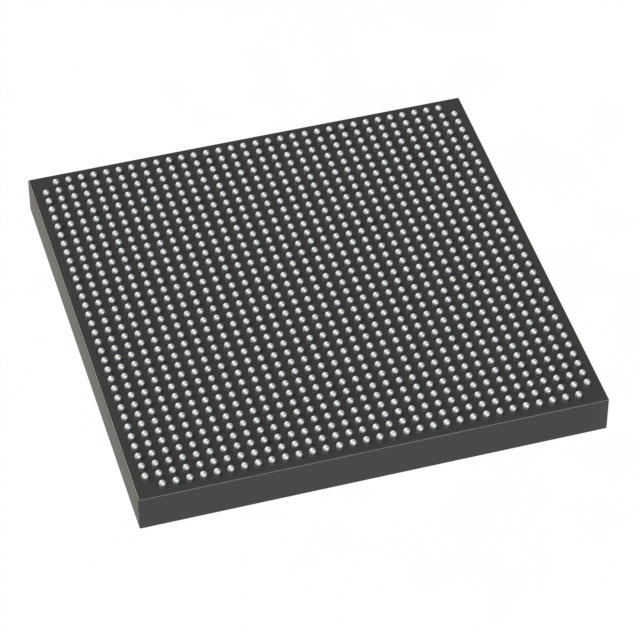
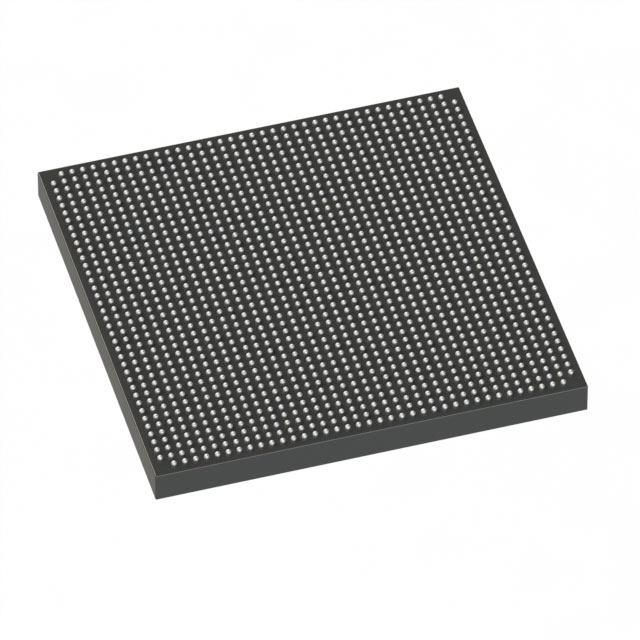
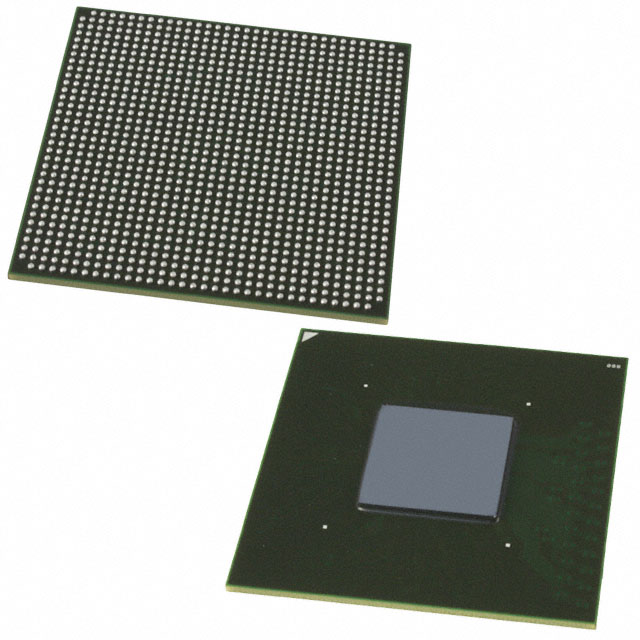
| Package / Case | 1152-BBGA, FCBGA | Number of I/O | 544 | Voltage | 1.07 V - 1.13 V | ||
| Mounting Method | Surface Mount | RoHS Compliance | RoHS Compliant | REACH Compliance | REACH Unaffected | ||
| Moisture Sensitivity Level | 3 (168 Hours) | Number of LABs/CLBs | 158491 | Number of Logic Elements/Cells | 420000 | ||
| Number of Gates | N/A | ECCN | N/A | HTS Code | N/A | ||
| Qualification | N/A | Total RAM Bits | 23625728 |
Overview of 5AGXMB5G6F35C6G – Arria V GX FPGA, 420,000 logic elements, 1152‑BBGA
The 5AGXMB5G6F35C6G is an Arria V GX Field Programmable Gate Array (FPGA) from Intel, delivered in a 1152‑ball BGA package for surface‑mount assembly. This commercial‑grade device integrates high logic density, extensive I/O, and embedded memory to address system designs that require programmable, high‑capacity digital resources.
With approximately 420,000 logic elements, 544 I/O pins and approximately 23.6 Mbits of on‑chip RAM, the device is suited to applications that need substantial programmable logic, abundant external connectivity, and on‑chip storage while operating within a commercial temperature range.
Key Features
- Logic Capacity Approximately 420,000 logic elements to implement complex custom logic, datapaths, and control logic in a single device.
- Embedded Memory Approximately 23.6 Mbits of embedded RAM for buffering, on‑chip storage and intermediate data processing.
- I/O and Connectivity 544 I/O pins provide broad external interfacing options for parallel buses, memory interfaces, sensors and peripherals.
- Package and Mounting 1152‑BBGA (FCBGA) package / supplier device package listed as 1152‑FBGA, FC (35×35); surface‑mountable for standard PCB assembly workflows.
- Power Specified core voltage supply range of 1.07 V to 1.13 V to guide power‑supply design and decoupling requirements.
- Thermal and Grade Commercial operating temperature range from 0 °C to 85 °C and commercial grade designation.
- Compliance RoHS compliant to support regulatory requirements for lead‑free assembly.
Typical Applications
- High‑density digital processing Use the device where large programmable logic fabric and on‑chip RAM are required for custom data processing and algorithm acceleration.
- Interface bridging and I/O expansion Leverage the 544 I/O pins to implement complex protocol bridging, multi‑lane interfaces or parallel peripheral control.
- System integration and prototyping Deploy as a central programmable fabric for integrating custom peripherals, glue logic and prototype systems on compact BGA footprint.
- Embedded control and coordination Implement system sequencers, control logic and timing managers that benefit from abundant logic and local RAM.
Unique Advantages
- High programmable density: The approximately 420,000 logic elements enable implementation of large, integrated digital designs without partitioning across multiple devices.
- Substantial on‑chip memory: Approximately 23.6 Mbits of embedded RAM reduces external memory dependency for many buffering and state‑storage tasks.
- Extensive I/O availability: 544 I/O pins simplify board‑level integration by providing capacity for multiple interfaces and peripherals directly to the FPGA.
- Industry vendor backing: Manufactured by Intel and based on the Arria V GX family architecture, providing consistent device specification and documented electrical/operational guidance.
- Package options for dense PCBs: 1152‑BBGA (35×35) package supports compact, high‑density board layouts suitable for space‑constrained systems.
- Regulatory readiness: RoHS compliance supports lead‑free manufacturing requirements.
Why Choose 5AGXMB5G6F35C6G?
The 5AGXMB5G6F35C6G Arria V GX FPGA positions itself as a high‑capacity, commercially rated programmable device for designs that demand significant logic resources, extensive I/O and meaningful on‑chip RAM. Its package and electrical envelope support integration into modern surface‑mounted PCB assemblies while providing the predictable operating and power parameters system designers require.
This device is appropriate for engineering teams building scalable digital systems, prototype platforms, or integrated controllers that benefit from large programmable fabric combined with a sizeable embedded memory and broad connectivity, all backed by Intel’s Arria V device documentation.
Request a quote or submit an inquiry to obtain pricing, availability and lead‑time information for the 5AGXMB5G6F35C6G Arria V GX FPGA.


Date Founded: 1968
Headquarters: Santa Clara, California, USA
Employees: 130,000+
Revenue: $54.23 Billion
Certifications and Memberships: ISO9001:2015, ISO14001:2015, ISO17025:2017, ISO27001:2022, ISO45001:2018, ISO50001:2018


