
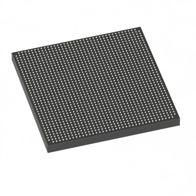
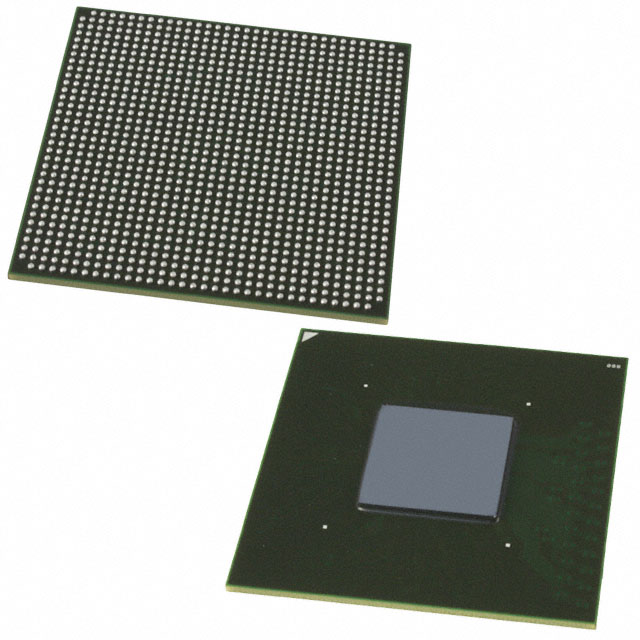
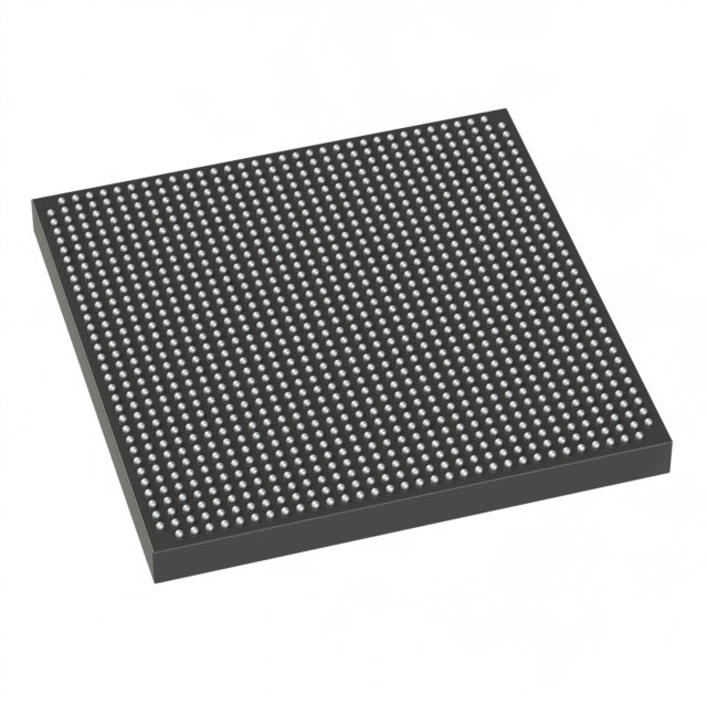
5AGXMB5G6F40C6N
| Part Description |
Arria V GX Field Programmable Gate Array (FPGA) IC 704 23625728 420000 1517-BBGA |
|---|---|
| Quantity | 1,171 Available (as of June 15, 2026) |

| Product Category | Field Programmable Gate Array (FPGA) |
|---|---|
| Manufacturer | Intel |
| Manufacturing Status | Obsolete |
| Manufacturer Standard Lead Time | Contact Us |
| Datasheet |
Specifications & Environmental
| Device Package | 1517-FBGA (40x40) | Grade | Commercial | Operating Temperature | 0°C – 85°C | ||
|---|---|---|---|---|---|---|---|
| Package / Case | 1517-BBGA | Number of I/O | 704 | Voltage | 1.07 V - 1.13 V | ||
| Mounting Method | Surface Mount | RoHS Compliance | RoHS Compliant | REACH Compliance | REACH Unknown | ||
| Moisture Sensitivity Level | 3 (168 Hours) | Number of LABs/CLBs | 19811 | Number of Logic Elements/Cells | 420000 | ||
| Number of Gates | N/A | ECCN | 3A001A2C | HTS Code | 8542.39.0001 | ||
| Qualification | N/A | Total RAM Bits | 23625728 |
Overview of 5AGXMB5G6F40C6N – Arria V GX FPGA, 420,000 logic elements, ~23.6 Mbits RAM, 704 I/Os, 1517‑BBGA
The 5AGXMB5G6F40C6N is an Intel Arria V GX field programmable gate array (FPGA) offered in a commercial-grade 1517‑BBGA package. It provides a high-density programmable fabric with 420,000 logic elements and extensive I/O capability for applications that require significant on-chip logic and memory integration.
With approximately 23.6 Mbits of embedded memory, 704 user I/Os, and a tightly specified core voltage range, this device targets designs that need dense logic, substantial embedded RAM, and a high pin count in a surface-mount BGA form factor.
Key Features
- High-density logic — 420,000 logic elements to implement complex programmable logic and custom hardware acceleration.
- Embedded memory — approximately 23.6 Mbits of on-chip RAM to support large buffer, cache, and data-path requirements without external memory for many functions.
- Extensive I/O — 704 user I/Os enabling wide parallel interfaces and high pin-count system integration.
- Package and mounting — supplied in a 1517‑BBGA package (supplier device package 1517‑FBGA, 40×40) designed for surface-mount assembly.
- Powering — specified core voltage range of 1.07 V to 1.13 V for predictable power delivery and integration into regulated power domains.
- Operating range — commercial temperature grade with specified operating range of 0 °C to 85 °C.
- Regulatory compliance — RoHS compliant.
Typical Applications
- High-density logic implementations: Designs that require substantial programmable logic capacity can leverage the 420,000 logic elements to implement complex state machines, datapaths, and custom accelerators.
- I/O‑intensive systems: Systems needing many parallel interfaces or large numbers of signals can use the 704 user I/Os for broad peripheral and board-level connectivity.
- Embedded memory-centric functions: Applications that benefit from significant on-chip memory, such as buffering, FIFOs, and on-chip caches, can leverage the device’s approximately 23.6 Mbits of embedded RAM.
- Compact, high-pin-count designs: The 1517‑BBGA surface-mount package supports compact PCB layouts while retaining high I/O density for space-constrained systems.
Unique Advantages
- Large programmable fabric: 420,000 logic elements provide the capacity to consolidate multiple functions into a single FPGA, reducing system component count.
- Substantial on-chip memory: Approximately 23.6 Mbits of embedded RAM reduces dependence on external memory for many data-path and buffering needs, simplifying board design.
- High I/O availability: 704 I/Os enable flexible interfacing options—parallel buses, wide data paths, and numerous peripheral connections—without external I/O expanders.
- Defined power envelope: A narrow supply range (1.07 V–1.13 V) supports stable core operation and predictable power budgeting in regulated designs.
- Commercial temperature rating: Rated for 0 °C to 85 °C to match a wide range of consumer and general-purpose applications.
- RoHS compliance: Meets RoHS requirements for environmental and manufacturing considerations.
Why Choose 5AGXMB5G6F40C6N?
The 5AGXMB5G6F40C6N Arria V GX FPGA balances high logic capacity, significant embedded memory, and a large I/O count in a compact 1517‑BBGA surface-mount package. It is suited to designers who need to integrate complex programmable logic, memory-rich functions, and extensive board-level interfacing while maintaining predictable power and thermal characteristics within a commercial operating range.
Because the device is RoHS compliant and supplied by Intel, it offers a verifiable specification set for procurement and design planning. Its combination of 420,000 logic elements, ~23.6 Mbits of embedded RAM, and 704 I/Os makes it a strong candidate for consolidating multi-chip designs into a single programmable device, reducing BOM and simplifying system architecture.
Request a quote or submit an inquiry to obtain pricing, lead-time, and availability information for 5AGXMB5G6F40C6N. Provide your requirements and our team will respond with a tailored quote.


Date Founded: 1968
Headquarters: Santa Clara, California, USA
Employees: 130,000+
Revenue: $54.23 Billion
Certifications and Memberships: ISO9001:2015, ISO14001:2015, ISO17025:2017, ISO27001:2022, ISO45001:2018, ISO50001:2018


