
5AGXMB7G4F35C5G
| Part Description |
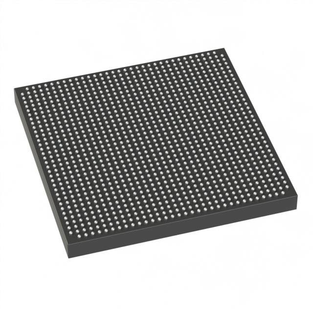
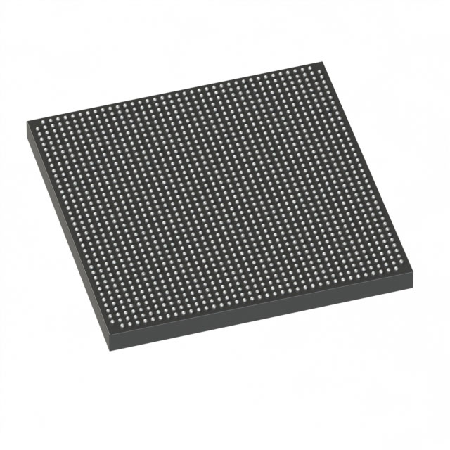
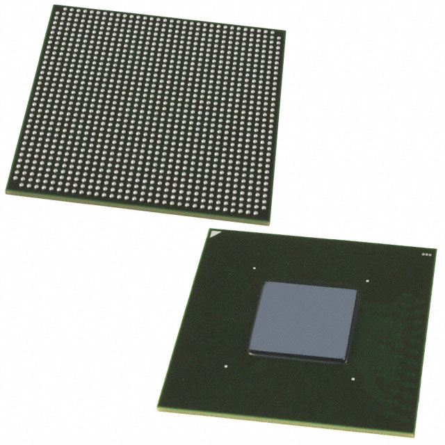
Arria V GX Field Programmable Gate Array (FPGA) IC 544 2975744 504140 1152-BBGA, FCBGA |
|---|---|
| Quantity | 534 Available (as of June 14, 2026) |
| Product Category | Field Programmable Gate Array (FPGA) |
|---|---|
| Manufacturer | Intel |
| Manufacturing Status | Active |
| Manufacturer Standard Lead Time | 16 Weeks |
| Datasheet |
Specifications & Environmental
| Device Package | 1152-FBGA, FC (35x35) | Grade | Commercial | Operating Temperature | 0°C – 85°C | ||
|---|---|---|---|---|---|---|---|
| Package / Case | 1152-BBGA, FCBGA | Number of I/O | 544 | Voltage | 1.07 V - 1.13 V | ||
| Mounting Method | Surface Mount | RoHS Compliance | RoHS Compliant | REACH Compliance | REACH Unaffected | ||
| Moisture Sensitivity Level | 3 (168 Hours) | Number of LABs/CLBs | 23786 | Number of Logic Elements/Cells | 504140 | ||
| Number of Gates | N/A | ECCN | N/A | HTS Code | N/A | ||
| Qualification | N/A | Total RAM Bits | 2975744 |
Overview of 5AGXMB7G4F35C5G – Arria V GX FPGA, 504,140 logic elements
The 5AGXMB7G4F35C5G is an Intel Arria V GX Field Programmable Gate Array (FPGA) in a 1152‑BBGA FCBGA package. It delivers a high logic capacity device with extensive on‑chip memory and a large I/O count suitable for commercial‑grade embedded designs.
With 504,140 logic elements, approximately 2.98 Mbits of embedded memory, and 544 I/O, this Arria V GX device targets applications that require high logic density, substantial local RAM and broad I/O connectivity while operating within a commercial temperature range.
Key Features
- Core Logic 504,140 logic elements provide large-scale programmable logic for complex digital designs and algorithm implementation.
- Embedded Memory Total on‑chip RAM of approximately 2.98 Mbits to support buffering, state storage and local data processing.
- I/O Capacity 544 available I/O pins to interface with wide peripheral arrays, data converters, and board‑level interconnects.
- Package 1152‑BBGA (FCBGA) supplier device package (1152‑FBGA, FC, 35×35) for high‑density board integration and reliable surface‑mount assembly.
- Power Supply Core voltage supply specified between 1.07 V and 1.13 V, enabling defined power provisioning for the FPGA core.
- Operating Conditions Commercial grade operation across 0 °C to 85 °C for typical commercial deployments.
- Compliance RoHS compliant construction for environmental regulatory alignment.
Typical Applications
- High‑density digital processing Architectures that require large amounts of programmable logic and embedded RAM benefit from the 504,140 logic elements and ≈2.98 Mbits of on‑chip memory.
- I/O‑intensive systems Platforms needing broad external connectivity can leverage the device’s 544 I/O pins for parallel interfaces, peripheral expansion, and board‑level routing.
- Commercial embedded systems Commercial‑grade designs operating within 0 °C to 85 °C can use this Arria V GX FPGA for compute and control tasks where high logic density is required.
Unique Advantages
- High logic and memory integration: Combines 504,140 logic elements with approximately 2.98 Mbits of embedded RAM to reduce external memory needs and speed local processing.
- Extensive I/O availability: 544 I/O pins provide flexibility for multi‑channel interfaces and complex board designs without immediate need for additional multiplexing logic.
- Industry‑standard BGA package: The 1152‑BBGA FCBGA package offers dense pinout and proven surface‑mount mounting for compact, high‑density PCBs.
- Defined core power window: A tightly specified core voltage range (1.07–1.13 V) simplifies power delivery planning and helps ensure consistent device operation.
- Commercial deployment ready: Rated for 0 °C to 85 °C operation and RoHS compliant to meet common commercial market requirements.
Why Choose 5AGXMB7G4F35C5G?
The 5AGXMB7G4F35C5G Arria V GX FPGA from Intel delivers a combination of high logic density, substantial embedded memory and broad I/O in a compact 1152‑BBGA package. Its commercial‑grade temperature rating and RoHS compliance make it suitable for production systems that demand predictable, high‑capacity programmable logic resources.
This part is suited for design teams that need to consolidate functions into a single, high‑density FPGA—reducing board complexity while maintaining flexibility for future design iterations. The device’s defined electrical and package characteristics support scalable designs and predictable integration into commercial product platforms.
Request a quote or submit a pricing and availability inquiry to receive part availability, lead time and ordering information for 5AGXMB7G4F35C5G.


Date Founded: 1968
Headquarters: Santa Clara, California, USA
Employees: 130,000+
Revenue: $54.23 Billion
Certifications and Memberships: ISO9001:2015, ISO14001:2015, ISO17025:2017, ISO27001:2022, ISO45001:2018, ISO50001:2018


