
5AGXMB7G6F35C6G
| Part Description |
Arria V GX Field Programmable Gate Array (FPGA) IC 544 2975744 504140 1152-BBGA, FCBGA |
|---|---|
| Quantity | 179 Available (as of June 15, 2026) |
| Product Category | Field Programmable Gate Array (FPGA) |
|---|---|
| Manufacturer | Intel |
| Manufacturing Status | Active |
| Manufacturer Standard Lead Time | 16 Weeks |
| Datasheet |
Specifications & Environmental
| Device Package | 1152-FBGA, FC (35x35) | Grade | Commercial | Operating Temperature | 0°C – 85°C | ||
|---|---|---|---|---|---|---|---|
| Package / Case | 1152-BBGA, FCBGA | Number of I/O | 544 | Voltage | 1.07 V - 1.13 V | ||
| Mounting Method | Surface Mount | RoHS Compliance | RoHS Compliant | REACH Compliance | REACH Unaffected | ||
| Moisture Sensitivity Level | 3 (168 Hours) | Number of LABs/CLBs | 23786 | Number of Logic Elements/Cells | 504140 | ||
| Number of Gates | N/A | ECCN | N/A | HTS Code | N/A | ||
| Qualification | N/A | Total RAM Bits | 2975744 |
Overview of 5AGXMB7G6F35C6G – Arria V GX Field Programmable Gate Array (FPGA)
The 5AGXMB7G6F35C6G is an Arria V GX family FPGA in a 1152-ball BGA FCBGA package, offering high logic density and extensive I/O for complex digital designs. With 504,140 logic elements and approximately 2.98 Mbits of embedded RAM, this commercial‑grade device targets designs that require large programmable logic capacity, substantial on-chip memory, and broad interfacing options.
Key Features
- Core Logic — 504,140 logic elements deliver substantial programmable logic capacity for complex control, signal processing, and custom hardware acceleration functions.
- Embedded Memory — Approximately 2.98 Mbits of on‑chip RAM to support buffering, FIFOs, and local data storage without external memory for many use cases.
- High I/O Count — 544 dedicated I/O pins to support wide parallel interfaces and dense connectivity to external peripherals and subsystems.
- Power Supply Range — Core voltage supply specified from 1.07 V to 1.13 V to match required power rails and board power sequencing.
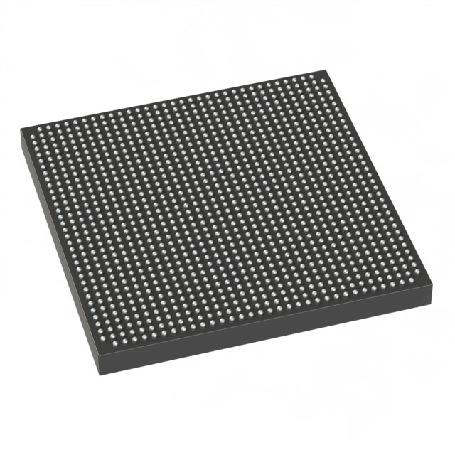
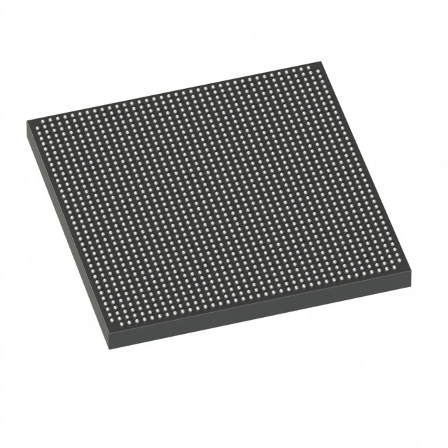
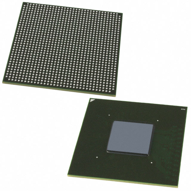
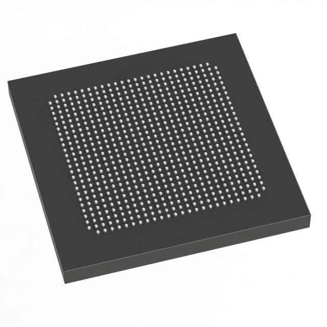
- Package & Mounting — 1152‑BBGA (FCBGA) package, supplier package 1152‑FBGA FC (35×35), designed for surface‑mount assembly in compact, high‑density system boards.
- Commercial Grade Temperature — Rated for operation from 0 °C to 85 °C for commercial deployments.
- Environmental Compliance — RoHS compliant for use in lead‑free manufacturing processes.
Typical Applications
- High‑density digital processing: Implement complex logic functions, custom datapaths, and hardware accelerators that require large numbers of logic elements and local memory.
- I/O‑intensive systems: Connect to multiple parallel buses, sensors, or peripherals using the device’s 544 I/O pins for flexible board-level interfacing.
- Embedded buffering and control: Use the on‑chip RAM for packet buffering, FIFOs, and local state storage in communication and control systems.
Unique Advantages
- High programmable density: 504,140 logic elements provide the capacity to consolidate multiple functions into a single FPGA, reducing external logic and board complexity.
- Significant on‑chip memory: Approximately 2.98 Mbits of embedded RAM minimizes dependence on external memory for mid‑size buffering and local storage.
- Extensive I/O resources: 544 I/O pins support complex interfacing and multi‑lane connectivity without immediate need for additional I/O expanders.
- Compact surface‑mount package: 1152‑ball FCBGA package supports high‑density PCB integration while maintaining a small board footprint.
- Commercial temperature and RoHS compliant: Rated for 0 °C to 85 °C operation and RoHS compliance to meet standard commercial manufacturing and environmental requirements.
Why Choose 5AGXMB7G6F35C6G?
The 5AGXMB7G6F35C6G Arria V GX FPGA combines a large logic fabric with substantial on‑chip memory and broad I/O in a compact FCBGA package, making it suitable for designs that demand high integration and flexible interfacing within commercial temperature ranges. It is well suited to engineers consolidating multiple functions into a single programmable device to reduce board complexity and part count.
Detailed electrical and configuration specifications for Arria V devices are available in the device datasheet, enabling precise system design and power sequencing based on the device’s operating and timing characteristics.
Request a quote or submit a product inquiry to obtain pricing, availability, and lead‑time details for the 5AGXMB7G6F35C6G Arria V GX FPGA.


Date Founded: 1968
Headquarters: Santa Clara, California, USA
Employees: 130,000+
Revenue: $54.23 Billion
Certifications and Memberships: ISO9001:2015, ISO14001:2015, ISO17025:2017, ISO27001:2022, ISO45001:2018, ISO50001:2018


