
5AGXMB7G6F35C6N
| Part Description |
Arria V GX Field Programmable Gate Array (FPGA) IC 544 27695104 504000 1152-BBGA, FCBGA Exposed Pad |
|---|---|
| Quantity | 1,214 Available (as of June 18, 2026) |
| Product Category | Field Programmable Gate Array (FPGA) |
|---|---|
| Manufacturer | Intel |
| Manufacturing Status | Obsolete |
| Manufacturer Standard Lead Time | Contact Us |
| Datasheet |
Specifications & Environmental
| Device Package | 1152-FBGA (35x35) | Grade | Commercial | Operating Temperature | 0°C – 85°C | ||
|---|---|---|---|---|---|---|---|
| Package / Case | 1152-BBGA, FCBGA Exposed Pad | Number of I/O | 544 | Voltage | 1.07 V - 1.13 V | ||
| Mounting Method | Surface Mount | RoHS Compliance | RoHS Compliant | REACH Compliance | REACH Unknown | ||
| Moisture Sensitivity Level | 3 (168 Hours) | Number of LABs/CLBs | 23780 | Number of Logic Elements/Cells | 504000 | ||
| Number of Gates | N/A | ECCN | 3A001A2C | HTS Code | 8542.39.0001 | ||
| Qualification | N/A | Total RAM Bits | 27695104 |
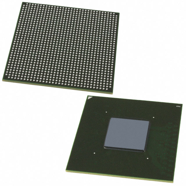
Overview of 5AGXMB7G6F35C6N – Arria V GX FPGA, 504,000 logic elements, 544 I/O, 1152-BBGA
The 5AGXMB7G6F35C6N is an Intel Arria V GX field programmable gate array (FPGA) supplied in a 1152-BBGA exposed-pad FCBGA package for surface-mount assembly. It delivers a high logic capacity and abundant I/O in a commercial-grade device.
With 504,000 logic elements and approximately 27.7 Mbits of embedded RAM, this device is targeted at designs that require dense logic integration, substantial on-chip memory, and a high pin count, while operating within standard commercial temperature and supply ranges.
Key Features
- Core Logic Capacity — 504,000 logic elements (cells) to support large-scale programmable logic implementations.
- Embedded Memory — Approximately 27.7 Mbits of on-chip RAM for buffering, LUT-based storage, and memory-mapped functions.
- I/O Density — 544 user I/O pins to accommodate wide bus interfaces and multiple external peripherals.
- Power and Voltage — Core voltage supply specified between 1.07 V and 1.13 V, enabling predictable power delivery design.
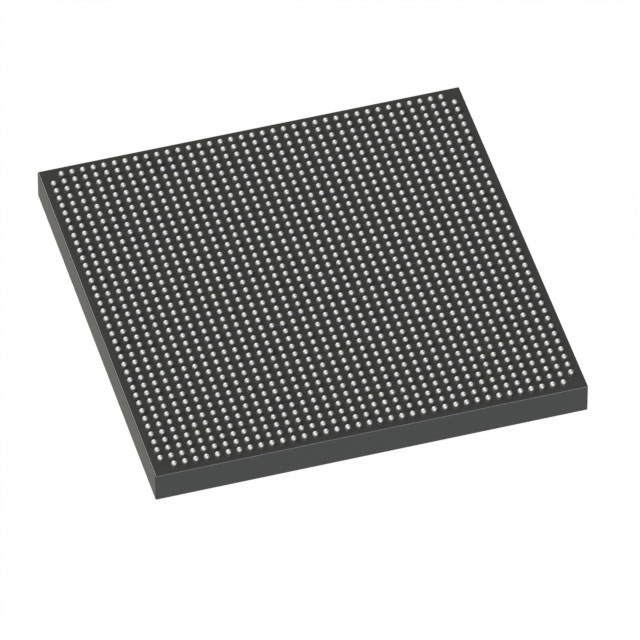
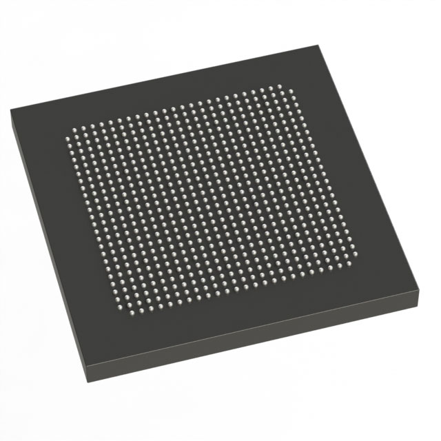
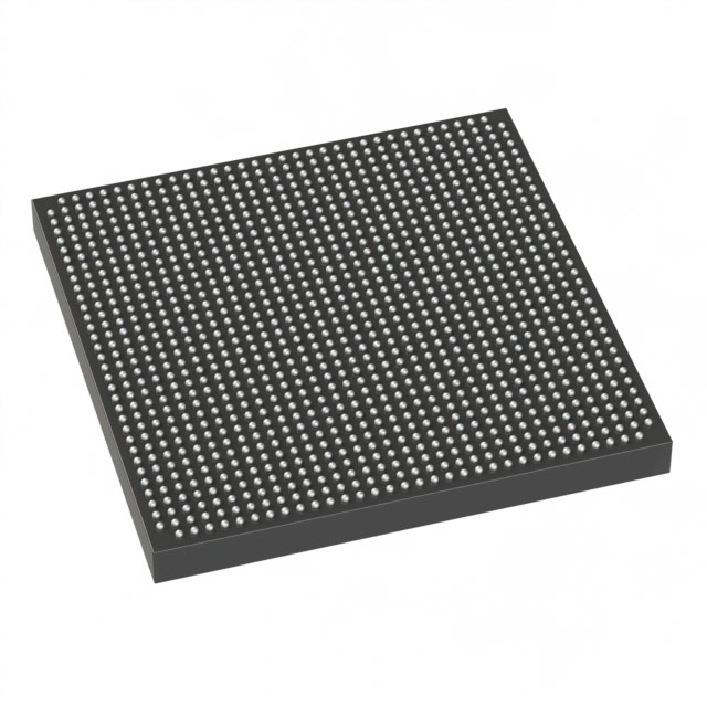
- Package & Mounting — 1152-BBGA, FCBGA exposed pad package (supplier device package: 1152-FBGA, 35×35 mm) with surface-mount mounting for compact board layouts and thermal contact.
- Operating Conditions — Commercial-grade device rated for 0°C to 85°C ambient operation.
- Standards Compliance — RoHS compliant, supporting regulatory-driven designs.
- Documented Device Characteristics — Detailed electrical, switching, configuration, and I/O timing specifications are provided in the Arria V device datasheet for GX-class devices.
Typical Applications
- I/O-Intensive Systems — Use the 544 I/O pins for designs that require multiple parallel interfaces, wide buses, or extensive sensor and peripheral connectivity.
- Memory-Centric Logic — Leverage approximately 27.7 Mbits of embedded RAM for buffering, packet storage, or local data processing without external memory.
- High-Logic-Density Designs — Deploy the 504,000 logic elements for complex finite-state machines, large combinatorial logic, or intensive control logic integration.
- Compact Surface-Mount Products — The 1152-BBGA exposed-pad FCBGA package supports compact PCB layouts with a thermal interface for efficient board-level heat dissipation.
Unique Advantages
- High Integration Density: 504,000 logic elements and substantial on-chip RAM reduce the need for external ASICs or discrete logic, simplifying BOM and board area.
- Generous I/O Count: 544 I/O pins enable multiple parallel interfaces and flexible system partitioning without external I/O expanders.
- Compact, Thermally Accessible Package: The exposed-pad 1152-BBGA FCBGA package facilitates thermal management in compact designs.
- Predictable Power Envelope: A defined supply range of 1.07 V to 1.13 V assists in power-supply design and system-level power budgeting.
- Commercial Temperature Qualified: Rated for 0°C to 85°C operation to meet standard commercial deployment requirements.
- Regulatory Compliance: RoHS compliance supports environmentally driven procurement and product requirements.
Why Choose 5AGXMB7G6F35C6N?
The 5AGXMB7G6F35C6N Arria V GX FPGA delivers a balance of high logic capacity, sizable embedded memory, and a large I/O complement in a surface-mount FCBGA package. Its specification set—504,000 logic elements, approximately 27.7 Mbits of on-chip RAM, 544 I/O, and a defined supply and temperature window—makes it a straightforward choice for commercial designs that demand dense programmable logic and extensive external connectivity.
Choose this device when your design requires significant on-chip resources, clear electrical and timing documentation, and RoHS compliance. It is well suited for engineering teams and procurement focused on scalable, high-density programmable solutions backed by documented device characteristics in the Arria V datasheet.
Request a quote or submit an inquiry to obtain pricing, availability, and technical support for the 5AGXMB7G6F35C6N Arria V GX FPGA.


Date Founded: 1968
Headquarters: Santa Clara, California, USA
Employees: 130,000+
Revenue: $54.23 Billion
Certifications and Memberships: ISO9001:2015, ISO14001:2015, ISO17025:2017, ISO27001:2022, ISO45001:2018, ISO50001:2018


