
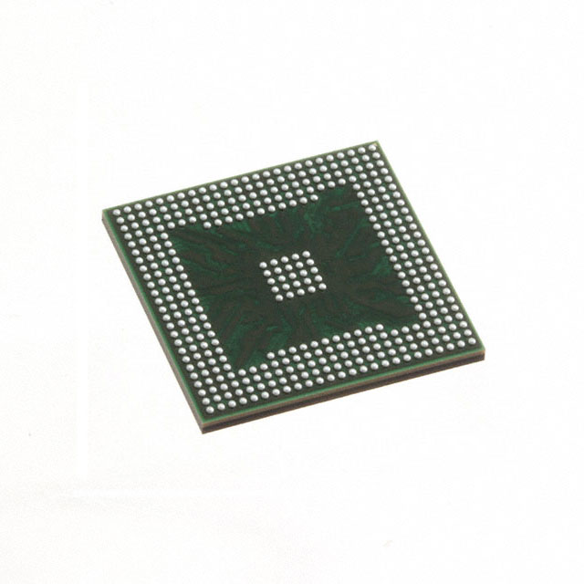
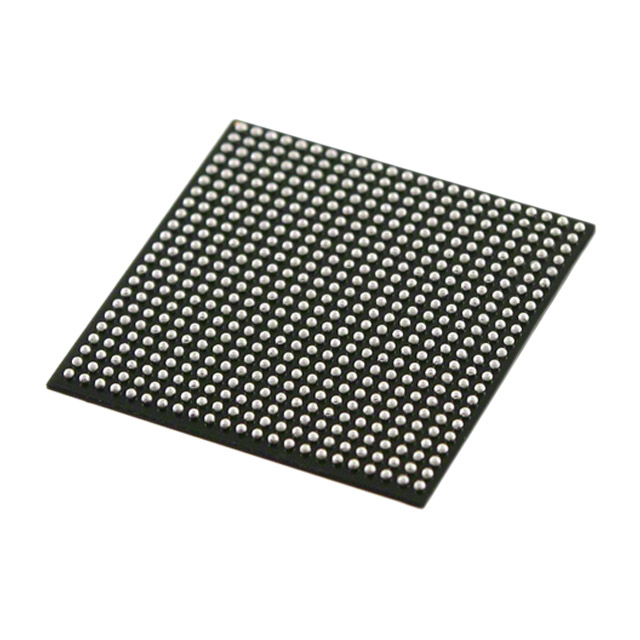
5CEFA4M13C7N
| Part Description |
Cyclone® V E Field Programmable Gate Array (FPGA) IC 223 3464192 49000 383-TFBGA |
|---|---|
| Quantity | 1,205 Available (as of June 15, 2026) |

| Product Category | Field Programmable Gate Array (FPGA) |
|---|---|
| Manufacturer | Intel |
| Manufacturing Status | Active |
| Manufacturer Standard Lead Time | 16 Weeks |
| Datasheet |
Specifications & Environmental
| Device Package | 383-MBGA (13x13) | Grade | Commercial | Operating Temperature | 0°C – 85°C | ||
|---|---|---|---|---|---|---|---|
| Package / Case | 383-TFBGA | Number of I/O | 223 | Voltage | 1.07 V - 1.13 V | ||
| Mounting Method | Surface Mount | RoHS Compliance | RoHS Compliant | REACH Compliance | REACH Unaffected | ||
| Moisture Sensitivity Level | 3 (168 Hours) | Number of LABs/CLBs | 18480 | Number of Logic Elements/Cells | 49000 | ||
| Number of Gates | N/A | ECCN | 3A001A2C | HTS Code | 8542.39.0001 | ||
| Qualification | N/A | Total RAM Bits | 3464192 |
Overview of 5CEFA4M13C7N – Cyclone® V E Field Programmable Gate Array (FPGA) IC, 49,000 logic elements, approx. 3.46 Mbits RAM, 223 I/O, 383-TFBGA
The 5CEFA4M13C7N is a Cyclone® V E series FPGA packaged in a 383-TFBGA (supplier package: 383-MBGA 13×13) surface-mount device. It combines a mid-density FPGA fabric with embedded memory and a broad I/O count to address cost-sensitive, high-volume embedded designs.
Built on a low-power 28 nm process and designed for a nominal 1.1 V core supply (device supply range 1.07 V to 1.13 V), this commercial-grade FPGA is intended for applications such as industrial, wireless and wireline communications, and military systems that need programmable logic, embedded memory, and flexible I/O integration.
Key Features
- Logic Capacity — 49,000 logic elements providing programmable fabric for glue logic, protocol handling, and custom datapaths.
- Embedded Memory — Approximately 3.46 Mbits of on-chip RAM to support buffering, packet processing, and local data storage.
- I/O Count — 223 general-purpose I/O pins for flexible peripheral, bus, and interface connections.
- Process and Core Voltage — Implemented on TSMC 28 nm low-power (28LP) process with a core supply range of 1.07 V to 1.13 V (nominal 1.1 V).
- Enhanced Logic Elements — Series-level features include an enhanced 8-input adaptive logic module (ALM) architecture for efficient logic packing and register use.
- DSP and Memory Architecture — Supports variable-precision DSP block functionality and embedded M10K memory block configurations (series feature), enabling efficient arithmetic and memory-intensive tasks.
- Package and Mounting — 383-TFBGA surface-mount package (supplier package: 383-MBGA 13×13) for compact board-level integration.
- Commercial Temperature Grade — Rated for 0 °C to 85 °C operation, suitable for commercial embedded applications.
- RoHS Compliant — Meets RoHS environmental requirements.
Typical Applications
- Industrial Control — Implement motor control loops, sensor aggregation, and deterministic I/O handling using the FPGA fabric and abundant I/O.
- Wireless and Wireline Communications — Use embedded memory and DSP-friendly logic to implement packet buffering, protocol processing, and intermediate signal processing stages.
- Defense and Test Equipment — Create configurable signal conditioning, custom processing pipelines, and real-time data handling leveraging on-chip RAM and logic density.
Unique Advantages
- Balanced Logic and Memory — 49,000 logic elements paired with approximately 3.46 Mbits of embedded memory enable mid-range designs that require both logic density and local storage.
- Low-Voltage, Low-Power Process — 28 nm low-power implementation and a narrow core supply range support efficient power usage in cost-sensitive designs.
- High I/O Density — 223 I/Os simplify integration with external peripherals, memory interfaces, and bus systems without excessive external glue logic.
- Compact Surface-Mount Package — 383-TFBGA (383-MBGA 13×13) helps minimize PCB area while supporting a robust pin count for system integration.
- Commercial Temperature Rating — 0 °C to 85 °C rating aligns with standard commercial embedded deployments.
- Environmentally Compliant — RoHS-compliant construction supports global manufacturing requirements.
Why Choose 5CEFA4M13C7N?
The 5CEFA4M13C7N offers a strong balance of programmable logic capacity, embedded memory, and high I/O count in a compact surface-mount package. Its 28 nm low-power foundation and narrow core voltage range make it suitable for designers targeting cost-sensitive, power-conscious applications that still require flexible on-board processing and interfacing.
This part is well suited for teams building mid-density FPGA solutions for industrial systems, communications equipment, and defense-related instruments that need reliable, programmable logic with on-chip memory and substantial I/O resources.
Request a quote or submit an inquiry to check availability and get pricing for 5CEFA4M13C7N. Our team can provide lead-time information and support for design planning.


Date Founded: 1968
Headquarters: Santa Clara, California, USA
Employees: 130,000+
Revenue: $54.23 Billion
Certifications and Memberships: ISO9001:2015, ISO14001:2015, ISO17025:2017, ISO27001:2022, ISO45001:2018, ISO50001:2018


