
5CGTFD5C5F27C7N
| Part Description |
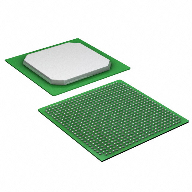
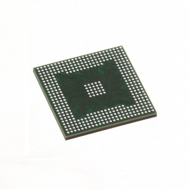
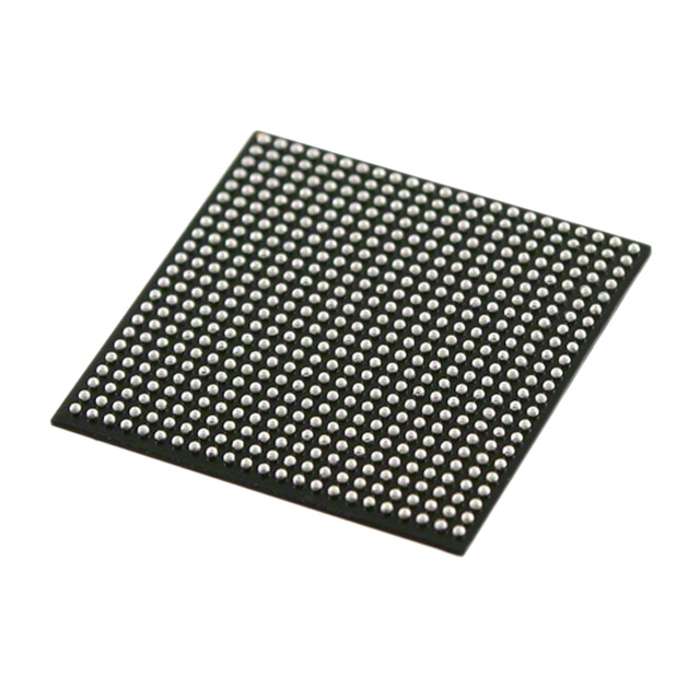
Cyclone® V GT Field Programmable Gate Array (FPGA) IC 336 5001216 77000 672-BGA |
|---|---|
| Quantity | 182 Available (as of June 15, 2026) |

| Product Category | Field Programmable Gate Array (FPGA) |
|---|---|
| Manufacturer | Intel |
| Manufacturing Status | Active |
| Manufacturer Standard Lead Time | 12 Weeks |
| Datasheet |
Specifications & Environmental
| Device Package | 672-FBGA (27x27) | Grade | Commercial | Operating Temperature | 0°C – 85°C | ||
|---|---|---|---|---|---|---|---|
| Package / Case | 672-BGA | Number of I/O | 336 | Voltage | 1.07 V - 1.13 V | ||
| Mounting Method | Surface Mount | RoHS Compliance | RoHS Compliant | REACH Compliance | REACH Unaffected | ||
| Moisture Sensitivity Level | 3 (168 Hours) | Number of LABs/CLBs | 29080 | Number of Logic Elements/Cells | 77000 | ||
| Number of Gates | N/A | ECCN | 3A991D | HTS Code | 8542.39.0001 | ||
| Qualification | N/A | Total RAM Bits | 5001216 |
Overview of 5CGTFD5C5F27C7N – Cyclone® V GT FPGA IC, 336 I/O, 672-BGA
The 5CGTFD5C5F27C7N is an Intel Cyclone® V GT field-programmable gate array supplied in a 672-ball BGA package. As a member of the Cyclone V family, this commercial-grade FPGA combines substantial programmable logic capacity with high I/O density and family-level integration features such as integrated transceivers and hard memory controllers.
With approximately 77,000 logic elements, roughly 5 Mbits of embedded memory, and 336 general-purpose I/Os, this device targets applications that require a balance of logic density, on-chip memory, and compact footprint while operating at a low core voltage.
Key Features
- Core logic Approximately 77,000 logic elements for implementing complex custom logic, control functions, and data-paths.
- Embedded memory Approximately 5 Mbits of on-chip RAM to support buffers, lookup tables, and local storage without immediate reliance on external memory.
- I/O and packaging 336 user I/Os in a compact 672-BGA (672-FBGA, 27×27) surface-mount package to maximize board-level connectivity in a small footprint.
- Power and voltage Core supply operating range of 1.07 V to 1.13 V; Cyclone V family devices are built on a 28 nm low-power (28LP) process to help reduce system power.
- Integrated system features Cyclone V devices are enhanced with integrated transceivers and hard memory controllers, enabling high-bandwidth interfaces and simplified external memory integration at the family level.
- Commercial-grade thermal range Rated for operation from 0 °C to 85 °C, suitable for commercial-environment deployments.
- RoHS compliant Device meets RoHS environmental requirements for lead-free manufacturing.
Typical Applications
- Wireless and wireline infrastructure High I/O count and family-level transceiver support suit PHY and protocol processing, fronthaul/backhaul, and data-path functions.
- Industrial systems Programmable logic and on-chip memory enable control, sensor aggregation, and custom I/O processing in automation equipment and machine control.
- Defense and communication equipment Logic density and integrated interface capabilities support custom processing, data buffering, and protocol adaptation in defense and specialized communications gear.
- Embedded compute and acceleration Logic elements and embedded RAM allow for offloading deterministic tasks, pre-processing, and custom accelerators within embedded platforms.
Unique Advantages
- High programmable density: Approximately 77,000 logic elements enable complex functions and substantial parallelism on-chip.
- On-chip memory for lower system cost: About 5 Mbits of embedded RAM reduces dependency on external memory for many buffering and control tasks.
- Flexible board-level integration: 336 I/Os in a compact 672-BGA package provide dense connectivity while conserving PCB area.
- Low-voltage operation: Narrow core-voltage window (1.07 V–1.13 V) and 28 nm low-power family technology help minimize core power consumption.
- Family-level interface IP: Cyclone V devices include integrated transceivers and hard memory controllers to streamline high-speed links and external memory interfaces.
- Commercial-ready and RoHS compliant: Designed for commercial-temperature operation (0 °C–85 °C) and RoHS-conformant production environments.
Why Choose 5CGTFD5C5F27C7N?
The 5CGTFD5C5F27C7N delivers a balance of logic capacity, embedded memory, and high I/O density in a compact 672-BGA package, making it a solid choice for designs that need sizeable programmable logic plus on-chip resources without a large board footprint. Its low-voltage operation and family-level integration features such as transceivers and hard memory controllers support efficient, high-bandwidth implementations while helping to control system cost and complexity.
This device is well suited to engineers and system designers building commercial-market communication, industrial, and defense-focused embedded systems who require programmable flexibility, built-in memory, and dense I/O in a single, RoHS-compliant device.
Request a quote or submit an RFQ to obtain pricing and availability information for the 5CGTFD5C5F27C7N.


Date Founded: 1968
Headquarters: Santa Clara, California, USA
Employees: 130,000+
Revenue: $54.23 Billion
Certifications and Memberships: ISO9001:2015, ISO14001:2015, ISO17025:2017, ISO27001:2022, ISO45001:2018, ISO50001:2018


