
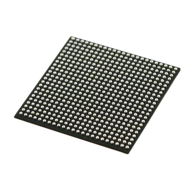
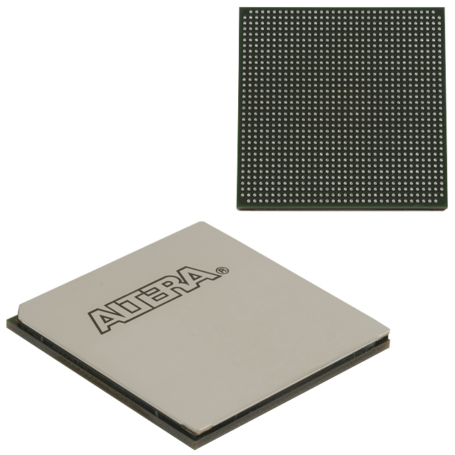
5CGXBC3B6U15C7N
| Part Description |
Cyclone® V GX Field Programmable Gate Array (FPGA) IC 144 1381376 31500 324-LFBGA |
|---|---|
| Quantity | 102 Available (as of June 18, 2026) |

| Product Category | Field Programmable Gate Array (FPGA) |
|---|---|
| Manufacturer | Intel |
| Manufacturing Status | Active |
| Manufacturer Standard Lead Time | 16 Weeks |
| Datasheet |
Specifications & Environmental
| Device Package | 324-UBGA (15x15) | Grade | Commercial | Operating Temperature | 0°C – 85°C | ||
|---|---|---|---|---|---|---|---|
| Package / Case | 324-LFBGA | Number of I/O | 144 | Voltage | 1.07 V - 1.13 V | ||
| Mounting Method | Surface Mount | RoHS Compliance | RoHS Compliant | REACH Compliance | REACH Unaffected | ||
| Moisture Sensitivity Level | 3 (168 Hours) | Number of LABs/CLBs | 11900 | Number of Logic Elements/Cells | 31500 | ||
| Number of Gates | N/A | ECCN | 3A991D | HTS Code | 8542.39.0001 | ||
| Qualification | N/A | Total RAM Bits | 1381376 |
Overview of 5CGXBC3B6U15C7N – Cyclone V GX FPGA, 31,500 logic elements, approximately 1.38 Mbits embedded memory, 144 I/Os, 324‑LFBGA
The 5CGXBC3B6U15C7N is an Intel Cyclone V GX field-programmable gate array (FPGA) in a 324‑LFBGA package. It pairs a cost-sensitive, low-power 28 nm FPGA fabric with the Cyclone V family’s integrated system features to address applications that require balanced logic density, embedded memory, and high-speed interfaces.
Targeted for industrial, wireless and wireline, and military applications, this GX variant combines on-chip resources and transceiver-ready architecture to support designs that need deterministic I/O, embedded memory, and compact packaging.
Key Features
- Core logic — 31,500 logic elements provide programmable fabric for glue logic, control, and mid-density digital processing.
- Embedded memory — Approximately 1.38 Mbits of on-chip RAM, delivered via Cyclone V memory blocks (M10K architectures are part of the device family), suitable for buffering, FIFOs, and small local datasets.
- DSP and compute — Support for variable-precision DSP blocks across the Cyclone V family enables efficient arithmetic and signal-processing implementations.
- High-speed I/O and transceivers — 144 general-purpose I/Os and GX family transceiver capability (Cyclone V family supports multi-gigabit transceivers) for interfacing to peripherals, memory, and communication links.
- Memory subsystem and controllers — Family-level hard memory controllers and external memory interface options simplify high-bandwidth connections to off-chip memories.
- Power and supply — Core supply operating range of 1.07 V to 1.13 V, matching the Cyclone V family’s low-voltage architecture for reduced power consumption.
- Package and mounting — Surface-mount 324‑LFBGA (supplier package: 324‑UBGA 15×15) provides a compact footprint for space-constrained boards.
- Operating range and compliance — Commercial-grade operating temperature of 0 °C to 85 °C and RoHS compliance for regulatory alignment.
Typical Applications
- Industrial control — Deterministic I/O and embedded memory make the device suitable for motor control, PLC auxiliary logic, and factory automation interfaces.
- Wireless infrastructure — GX transceiver capability and DSP resources support PHY front-end functions, protocol offload, and intermediate processing in wireless basestations and repeaters.
- Wireline communications — High-speed I/O, hard memory controllers, and on-chip RAM enable packet buffering, framing, and protocol bridging in wired network equipment.
- Military and avionics subsystems — Programmability and integrated interfaces support custom digital processing and data aggregation tasks in defense electronics where reconfigurability is required.
- Embedded SoC and prototyping — The Cyclone V family features (including optional HPS integration across the family) suit system prototyping and embedded processing tasks that combine software and programmable logic.
Unique Advantages
- Balanced logic density: 31,500 logic elements deliver mid-range capacity for control, protocol, and processing tasks without excessive board area or cost.
- On-chip memory for real-time buffering: Approximately 1.38 Mbits of embedded RAM supports FIFOs, small caches, and local data storage to reduce external memory traffic.
- Integrated transceiver and memory controller support: Family-level support for multi-gigabit transceivers and hard memory controllers streamlines high-bandwidth interface design.
- Low-voltage core operation: Core supply range of 1.07 V to 1.13 V aligns with low-power system requirements and simplifies power-rail planning.
- Compact BGA footprint: 324‑LFBGA (15×15 supplier UBGA) enables deployment in space-constrained PCBs while providing dense I/O.
- Commercial temperature and RoHS compliance: Rated for 0 °C to 85 °C operation and RoHS‑compliant to meet common commercial product requirements.
Why Choose 5CGXBC3B6U15C7N?
The 5CGXBC3B6U15C7N combines Cyclone V GX family features—mid-density logic, embedded memory, DSP resources, and transceiver-ready architecture—into a compact 324‑LFBGA package. It is designed for engineers building cost-sensitive, bandwidth-aware systems that benefit from on-chip memory and programmable logic.
This part is well suited for teams needing a balance of integration, predictable I/O capacity, and the flexibility of FPGA-based design. Backed by Intel's Cyclone V device family specifications, it offers a scalable option for prototyping and production where commercial temperature range and RoHS compliance are required.
Request a quote or submit an inquiry for pricing and availability to evaluate 5CGXBC3B6U15C7N for your next design project.


Date Founded: 1968
Headquarters: Santa Clara, California, USA
Employees: 130,000+
Revenue: $54.23 Billion
Certifications and Memberships: ISO9001:2015, ISO14001:2015, ISO17025:2017, ISO27001:2022, ISO45001:2018, ISO50001:2018


