
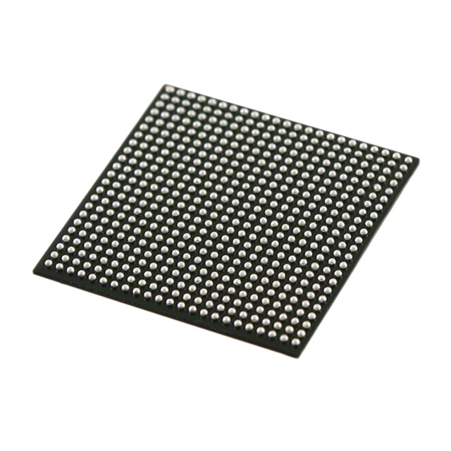
5CGXBC4C6F23C7N
| Part Description |
Cyclone® V GX Field Programmable Gate Array (FPGA) IC 240 2862080 50000 484-BGA |
|---|---|
| Quantity | 622 Available (as of June 14, 2026) |
| Product Category | Field Programmable Gate Array (FPGA) |
|---|---|
| Manufacturer | Intel |
| Manufacturing Status | Active |
| Manufacturer Standard Lead Time | 12 Weeks |
| Datasheet |
Specifications & Environmental
| Device Package | 484-FBGA (23x23) | Grade | Commercial | Operating Temperature | 0°C – 85°C | ||
|---|---|---|---|---|---|---|---|
| Package / Case | 484-BGA | Number of I/O | 240 | Voltage | 1.07 V - 1.13 V | ||
| Mounting Method | Surface Mount | RoHS Compliance | RoHS Compliant | REACH Compliance | REACH Unaffected | ||
| Moisture Sensitivity Level | 3 (168 Hours) | Number of LABs/CLBs | 18868 | Number of Logic Elements/Cells | 50000 | ||
| Number of Gates | N/A | ECCN | 3A991D | HTS Code | 8542.39.0001 | ||
| Qualification | N/A | Total RAM Bits | 2862080 |
Overview of 5CGXBC4C6F23C7N – Cyclone® V GX Field Programmable Gate Array (FPGA) IC 240 I/O 2.86 Mbit RAM 50k LE 484-BGA
The 5CGXBC4C6F23C7N is a Cyclone® V GX-series FPGA in a 484-ball FBGA package, designed for mid-density, cost-sensitive commercial applications. It combines programmable fabric, embedded memory, and a wide I/O complement to address industrial, wireless/wireline and communications designs that require a balance of logic capacity, on-chip RAM, and integrated high-speed interfaces.
Built on the Cyclone V device family architecture, this commercial-grade device targets systems that benefit from lower power operation, integrated transceivers and hard memory controllers while remaining simple to package and deploy in surface-mount assemblies.
Key Features
- Logic Capacity — 50,000 logic elements provide substantial programmable logic for mid-density designs and custom datapath implementation.
- Embedded Memory — Approximately 2.86 Mbits of on-chip RAM to support buffering, FIFOs, and local storage; the Cyclone V family also uses M10K memory blocks with soft ECC in its device architecture.
- I/O and Connectivity — 240 general-purpose I/O pins and the Cyclone V GX family’s integrated transceivers and hard memory controllers support a range of external interfaces and high-speed links.
- Process and Core Voltage — Device architecture uses a 28‑nm low‑power silicon process with a nominal 1.1 V core; this part specifies a supply range of 1.07 V to 1.13 V for core operation.
- Package and Mounting — Surface-mount 484-FBGA (23 × 23) package simplifies board integration while keeping a compact footprint.
- Operating Range — Commercial-grade operating temperature from 0 °C to 85 °C for standard commercial deployments.
- Environmental Compliance — RoHS-compliant construction to meet lead-free assembly requirements.
Typical Applications
- Industrial Control — Control logic, sensor aggregation and protocol bridging using on-chip memory and abundant logic elements for deterministic real-time processing.
- Wireless and Wireline Infrastructure — Baseband processing, packet handling and link interfacing that leverage integrated transceivers and hard memory controllers for high-throughput data paths.
- Communications and Defense Systems — Mid-density signal processing and custom protocol implementations that require a mix of logic, embedded RAM and flexible I/O.
Unique Advantages
- Balanced Integration: 50,000 logic elements and ~2.86 Mbits of embedded RAM provide a strong mix of logic and memory for mid-range FPGA designs, reducing the need for external SRAM in many use cases.
- High I/O Flexibility: 240 I/O pins plus integrated transceiver and hard memory controller capabilities support diverse interface requirements and simplify system-level connectivity.
- Low-Power Silicon: Built on a 28‑nm low‑power process with a 1.07–1.13 V core supply window, enabling efficient operation in power-sensitive commercial applications.
- Compact, Surface-Mount Package: 484-FBGA (23 × 23) packaging enables dense board layouts while maintaining mechanical compatibility with standard SMT assembly flows.
- Regulatory Readiness: RoHS compliance supports lead-free manufacturing and environmental requirements for commercial products.
Why Choose 5CGXBC4C6F23C7N?
This Cyclone V GX device offers a pragmatic combination of logic density, on-chip memory and a broad I/O set in a compact 484-FBGA package, making it well suited to commercial systems that require significant programmable logic and embedded RAM without moving to higher-cost device classes. The device’s 1.07–1.13 V supply window and commercial temperature rating align it with standard production environments.
Designers seeking a mid-density FPGA for industrial controls, communications infrastructure, or defense communications can leverage the Cyclone V architecture—featuring low-power process technology, embedded memory structures, and integrated transceiver/memory-controller capabilities—to simplify board-level design and accelerate time to market.
Request a quote or submit an inquiry for availability and pricing of 5CGXBC4C6F23C7N to evaluate this FPGA for your next design.


Date Founded: 1968
Headquarters: Santa Clara, California, USA
Employees: 130,000+
Revenue: $54.23 Billion
Certifications and Memberships: ISO9001:2015, ISO14001:2015, ISO17025:2017, ISO27001:2022, ISO45001:2018, ISO50001:2018


