
5CGXBC4C6U19C7N
| Part Description |
Cyclone® V GX Field Programmable Gate Array (FPGA) IC 224 2862080 50000 484-FBGA |
|---|---|
| Quantity | 362 Available (as of June 15, 2026) |

| Product Category | Field Programmable Gate Array (FPGA) |
|---|---|
| Manufacturer | Intel |
| Manufacturing Status | Active |
| Manufacturer Standard Lead Time | 12 Weeks |
| Datasheet |
Specifications & Environmental
| Device Package | 484-UBGA (19x19) | Grade | Commercial | Operating Temperature | 0°C – 85°C | ||
|---|---|---|---|---|---|---|---|
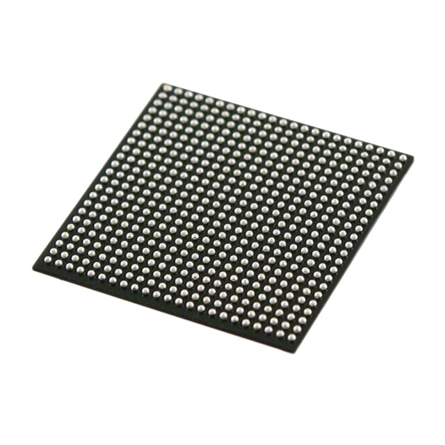
| Package / Case | 484-FBGA | Number of I/O | 224 | Voltage | 1.07 V - 1.13 V | ||
| Mounting Method | Surface Mount | RoHS Compliance | RoHS Compliant | REACH Compliance | REACH Unaffected | ||
| Moisture Sensitivity Level | 3 (168 Hours) | Number of LABs/CLBs | 18868 | Number of Logic Elements/Cells | 50000 | ||
| Number of Gates | N/A | ECCN | 3A991D | HTS Code | 8542.39.0001 | ||
| Qualification | N/A | Total RAM Bits | 2862080 |
Overview of 5CGXBC4C6U19C7N – Cyclone® V GX FPGA, 50,000 logic elements, 224 I/O, 484-FBGA
The 5CGXBC4C6U19C7N is an Intel Cyclone® V GX field programmable gate array (FPGA) in a 484-FBGA (484-UBGA 19×19) package. It delivers a balance of programmable logic, on-chip memory, and high I/O density for cost-sensitive, bandwidth-focused applications.
Built on TSMC's 28‑nm low‑power (28LP) process and aligned with the Cyclone V family architecture, this device targets industrial, wireless and wireline, and military application spaces where integration, predictable power characteristics, and board-level packing density matter.
Key Features
- Logic Capacity — Approximately 50,000 logic elements for implementing complex combinational and sequential logic.
- Embedded Memory — Approximately 2.86 Mbits of on-chip RAM (2,862,080 bits) to support buffering, FIFOs, and local storage.
- I/O Density — 224 general-purpose I/O pins to support wide parallel interfaces and multiple peripheral connections.
- Process and Power — Manufactured on TSMC 28‑nm low‑power (28LP) process; nominal core supply measured between 1.07 V and 1.13 V.
- Package & Mounting — 484‑FBGA package (supplier: 484‑UBGA, 19×19) designed for surface-mount assembly and compact board footprints.
- Operating Conditions — Commercial grade device with an operating temperature range of 0 °C to 85 °C.
- Standards Compliance — RoHS‑compliant to meet current environmental requirements.
- Cyclone V GX Family Attributes — Part of the Cyclone V GX family that emphasizes lower power, integrated transceivers, and hard memory controllers for bandwidth-oriented designs.
Typical Applications
- Industrial systems — FPGA fabric and embedded memory suitable for custom logic, data aggregation, and control functions in factory and process equipment.
- Wireless and wireline equipment — Architecture and family-level transceiver/hard-IP integration designed for communications hardware that requires efficient bandwidth handling.
- Military systems — Used where programmable logic and on-board memory support mission-specific processing (commercial-grade operating range applies).
Unique Advantages
- Balanced programmable capacity: Around 50,000 logic elements provide a mid-range FPGA fabric suitable for sizable custom logic implementations without excess cost.
- Significant on-chip RAM: Approximately 2.86 Mbits of embedded memory reduces reliance on external RAM for many buffering and local storage tasks, simplifying board design.
- High I/O count: 224 I/O pins enable broad peripheral and parallel interface support directly from the FPGA package.
- Low-power process: Built on 28‑nm low‑power technology with a nominal core supply near 1.1 V, supporting tighter power budgets in space-constrained systems.
- Compact, surface-mount packaging: 484‑FBGA (484‑UBGA, 19×19) provides a dense footprint for high-functionality boards where PCB real estate is at a premium.
- Regulatory hygiene: RoHS compliance facilitates integration into designs that require lead‑free manufacturing practices.
Why Choose 5CGXBC4C6U19C7N?
The 5CGXBC4C6U19C7N combines a Cyclone V GX architecture with a practical mix of logic, on‑chip memory, and high I/O count in a compact 484‑FBGA package. Its 28‑nm low‑power construction and documented core voltage window make it attractive for designs that require predictable power behavior and efficient integration of bandwidth-oriented functions.
This part suits engineering teams and procurement sourcing looking for a commercially graded FPGA that delivers mid-range logic capacity, meaningful embedded RAM, and the I/O resources needed for communications and industrial designs, while adhering to RoHS environmental requirements.
Request a quote or submit your requirements to receive pricing, availability, and ordering details for 5CGXBC4C6U19C7N.


Date Founded: 1968
Headquarters: Santa Clara, California, USA
Employees: 130,000+
Revenue: $54.23 Billion
Certifications and Memberships: ISO9001:2015, ISO14001:2015, ISO17025:2017, ISO27001:2022, ISO45001:2018, ISO50001:2018


