
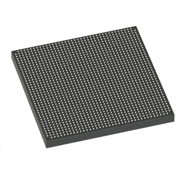
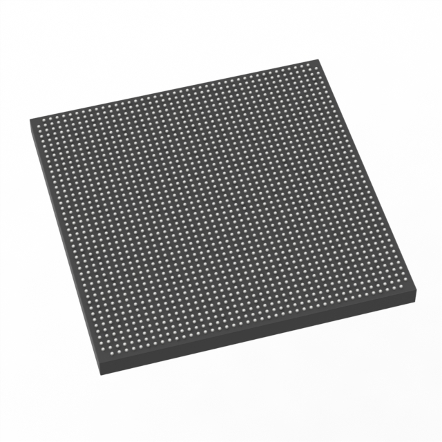
5SEEBH40C2LN
| Part Description |
Stratix® V E Field Programmable Gate Array (FPGA) IC 696 53248000 952000 1517-BBGA, FCBGA |
|---|---|
| Quantity | 237 Available (as of June 14, 2026) |
| Product Category | Field Programmable Gate Array (FPGA) |
|---|---|
| Manufacturer | Intel |
| Manufacturing Status | Obsolete |
| Manufacturer Standard Lead Time | Contact Us |
| Datasheet |
Specifications & Environmental
| Device Package | 1517-HBGA (45x45) | Grade | Commercial | Operating Temperature | 0°C – 85°C | ||
|---|---|---|---|---|---|---|---|
| Package / Case | 1517-BBGA, FCBGA | Number of I/O | 696 | Voltage | 820 mV - 880 mV | ||
| Mounting Method | Surface Mount | RoHS Compliance | RoHS Compliant | REACH Compliance | REACH Unknown | ||
| Moisture Sensitivity Level | 3 (168 Hours) | Number of LABs/CLBs | 359250 | Number of Logic Elements/Cells | 952000 | ||
| Number of Gates | N/A | ECCN | 3A001A2C | HTS Code | 8542.39.0001 | ||
| Qualification | N/A | Total RAM Bits | 53248000 |
Overview of 5SEEBH40C2LN – Stratix® V E Field Programmable Gate Array (FPGA)
The 5SEEBH40C2LN is a Stratix V E-series FPGA offering very-high logic capacity in a compact FCBGA package. Built on the Stratix V architecture, this device targets high-density, data- and compute-intensive applications such as system emulation, diagnostic imaging, and instrumentation.
With nearly one million logic elements, abundant embedded memory and a large I/O count, the device delivers a platform for complex, high-performance designs while supporting standard commercial temperature and supply environments.
Key Features
- High logic density: 952,000 logic elements provide the capacity for large, complex designs and system-level prototypes.
- Embedded memory: Approximately 53.25 Mbits of on-chip RAM (53,248,000 bits) to support data buffering, lookup tables, and state storage.
- Extensive I/O: 696 I/O pins for broad external interfacing and system connectivity.
- Process and core: Stratix V family architecture built on a 28‑nm TSMC process with core voltage options described in the device handbook; this device lists an operating supply window of 820 mV to 880 mV.
- Integrated hard IP options: Family features include Embedded HardCopy Blocks used for hardened IP instantiation (for example, PCIe Gen3/Gen2/Gen1 as described in the device documentation).
- Package and mounting: 1517‑BBGA FCBGA package (supplier package 1517‑HBGA, 45 × 45 mm) for surface‑mount PCB assembly.
- Commercial grade and temperature: Rated for commercial operation from 0 °C to 85 °C.
- Standards and compliance: RoHS compliant.
Typical Applications
- System emulation and prototyping: High logic element count and large embedded memory make the device suitable for hardware emulation and early silicon validation tasks.
- Diagnostic imaging: Large logic and memory resources support image processing pipelines, buffering, and complex algorithm acceleration.
- Instrumentation and test equipment: Extensive I/O and high integration enable flexible front-end interfaces and on-board data handling for measurement systems.
- ASIC prototyping and low-risk migration: Stratix V family features and Embedded HardCopy Blocks support prototyping paths toward hardened ASIC implementations as described in the device documentation.
Unique Advantages
- Massive on-chip capacity: Nearly one million logic elements reduce the need for multiple devices, simplifying system architecture and board design.
- Significant embedded memory: Approximately 53.25 Mbits of RAM enables large buffers and on-chip data staging, improving latency and throughput for data-intensive functions.
- Broad external connectivity: 696 I/O pins support diverse peripherals and parallel interfaces without compromising signal routing density.
- Compact, production-ready package: 1517‑BBGA/1517‑HBGA (45 × 45 mm) FCBGA package provides a high-pin-count solution in a standard form factor for surface-mount assembly.
- Commercial temperature rating and RoHS compliance: Suitable for mainstream commercial applications with regulatory compliance for lead‑free manufacturing.
- Design continuity within Stratix V family: Family-level features such as Embedded HardCopy Blocks and the 28‑nm architecture provide a clear migration path for higher-volume or hardened IP deployments.
Why Choose 5SEEBH40C2LN?
The 5SEEBH40C2LN combines very high logic density, substantial embedded memory and a large I/O complement in a single Stratix V E-series FPGA package. It is positioned for engineers who need on-chip capacity and flexible interfacing to implement complex algorithms, hardware emulation, or data-heavy processing tasks within commercial temperature ranges.
Choosing this device delivers a scalable platform backed by the Stratix V family architecture and device-level features described in the product documentation, helping teams move from prototyping to higher-volume implementations while maintaining design continuity.
Request a quote or submit an inquiry to check availability, lead times and pricing for 5SEEBH40C2LN.


Date Founded: 1968
Headquarters: Santa Clara, California, USA
Employees: 130,000+
Revenue: $54.23 Billion
Certifications and Memberships: ISO9001:2015, ISO14001:2015, ISO17025:2017, ISO27001:2022, ISO45001:2018, ISO50001:2018


