
5SGSMD4K2F40I3LG
| Part Description |
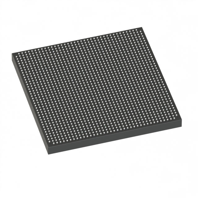
Stratix® V GS Field Programmable Gate Array (FPGA) IC 696 19456000 360000 1517-BBGA, FCBGA |
|---|---|
| Quantity | 52 Available (as of June 15, 2026) |

| Product Category | Field Programmable Gate Array (FPGA) |
|---|---|
| Manufacturer | Intel |
| Manufacturing Status | Active |
| Manufacturer Standard Lead Time | 26 Weeks |
| Datasheet |
Specifications & Environmental
| Device Package | 1517-FBGA (40x40) | Grade | Industrial | Operating Temperature | -40°C – 100°C | ||
|---|---|---|---|---|---|---|---|
| Package / Case | 1517-BBGA, FCBGA | Number of I/O | 696 | Voltage | 820 mV - 880 mV | ||
| Mounting Method | Surface Mount | RoHS Compliance | RoHS Compliant | REACH Compliance | REACH Unaffected | ||
| Moisture Sensitivity Level | 3 (168 Hours) | Number of LABs/CLBs | 135840 | Number of Logic Elements/Cells | 360000 | ||
| Number of Gates | N/A | ECCN | N/A | HTS Code | N/A | ||
| Qualification | N/A | Total RAM Bits | 19456000 |
Overview of 5SGSMD4K2F40I3LG – Stratix® V GS FPGA, 360,000 logic elements, 1517-FBGA
The 5SGSMD4K2F40I3LG is a Stratix® V GS Field Programmable Gate Array (FPGA) in a 1517-FBGA (40×40) package designed for industrial-temperature operation. It delivers a high logic density platform with extensive I/O and embedded memory for complex, system-level implementations where integration and predictable operating conditions matter.
Key architectural highlights for this device include 360,000 logic elements, approximately 19.46 Mbits of on-chip RAM, and up to 696 I/O pins, providing the resources required for compute-intensive and I/O-rich designs.
Key Features
- Logic Capacity – 360,000 logic elements and 135,840 logic array blocks (LABs) to implement large, high-density designs.
- Embedded Memory – Approximately 19.46 Mbits of total on-chip RAM to support buffering, packet processing, and large FPGA-resident data structures.
- I/O Resources – Up to 696 I/O pins for extensive external interfacing and high-channel-count system integration.
- Package & Mounting – 1517-BBGA / FCBGA package (Supplier device package: 1517-FBGA, 40×40) with surface-mount mounting for compact PCB integration.
- Power and Core Voltage – Core supply range from 820 mV to 880 mV, enabling designers to target low-voltage core operation as part of power budgeting.
- Industrial Temperature Grade – Rated for −40 °C to 100 °C operation to meet harsher environmental requirements.
- RoHS Compliant – Conforms to RoHS requirements for lead-free assembly and regulatory compliance.
Typical Applications
- High-density networking & switching – Large logic capacity and abundant I/O make this device suitable for packet processing, classification, and multi-port switching fabrics.
- Data center acceleration – Significant on-chip RAM and logic resources support hardware acceleration tasks and custom compute kernels.
- Video and broadcast processing – High logic density and extensive I/O enable multi-channel video pipelines and real-time processing engines.
- Industrial control & test equipment – Industrial temperature rating and robust I/O count support control systems and instrumentation in demanding environments.
Unique Advantages
- High logic density: 360,000 logic elements provide the capacity to consolidate multiple system functions into a single device, reducing board-level complexity.
- Large embedded memory: Approximately 19.46 Mbits of on-chip RAM minimizes external memory dependence for buffering and data-path implementations.
- Extensive connectivity: Up to 696 I/O pins enable broad peripheral and protocol support without immediate need for external I/O expanders.
- Industrial robustness: −40 °C to 100 °C operating range supports deployment in temperature-challenging installations.
- Compact system footprint: 1517-FBGA (40×40) package and surface-mount mounting allow dense PCB layouts for space-constrained designs.
- Regulatory readiness: RoHS compliance supports modern assembly and environmental requirements.
Why Choose 5SGSMD4K2F40I3LG?
The 5SGSMD4K2F40I3LG positions itself as a high-capacity Stratix V GS FPGA option for engineers who require substantial logic, on-chip memory, and wide I/O in an industrial temperature-rated device. Its combination of 360,000 logic elements, approximately 19.46 Mbits of embedded RAM, and 696 I/Os enables consolidation of complex functions and reduces system bill of materials.
This device is well suited to designs that demand scalable compute resources and predictable operating behavior across −40 °C to 100 °C. For teams designing networking, acceleration, video processing, or industrial control systems, the 5SGSMD4K2F40I3LG provides a compact, RoHS-compliant FPGA foundation with a proven Stratix V architecture.
Request a quote or submit an inquiry to evaluate 5SGSMD4K2F40I3LG for your next design and to obtain pricing and availability information.


Date Founded: 1968
Headquarters: Santa Clara, California, USA
Employees: 130,000+
Revenue: $54.23 Billion
Certifications and Memberships: ISO9001:2015, ISO14001:2015, ISO17025:2017, ISO27001:2022, ISO45001:2018, ISO50001:2018


