
5SGSMD6K2F40C3G
| Part Description |
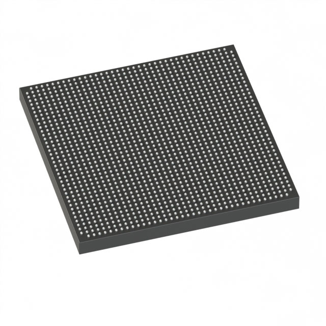
Stratix® V GS Field Programmable Gate Array (FPGA) IC 696 46080000 583000 1517-BBGA, FCBGA |
|---|---|
| Quantity | 590 Available (as of June 16, 2026) |

| Product Category | Field Programmable Gate Array (FPGA) |
|---|---|
| Manufacturer | Intel |
| Manufacturing Status | Active |
| Manufacturer Standard Lead Time | 26 Weeks |
| Datasheet |
Specifications & Environmental
| Device Package | 1517-FBGA (40x40) | Grade | Commercial | Operating Temperature | 0°C – 85°C | ||
|---|---|---|---|---|---|---|---|
| Package / Case | 1517-BBGA, FCBGA | Number of I/O | 696 | Voltage | 820 mV - 880 mV | ||
| Mounting Method | Surface Mount | RoHS Compliance | RoHS Compliant | REACH Compliance | REACH Unaffected | ||
| Moisture Sensitivity Level | 3 (168 Hours) | Number of LABs/CLBs | 220000 | Number of Logic Elements/Cells | 583000 | ||
| Number of Gates | N/A | ECCN | N/A | HTS Code | N/A | ||
| Qualification | N/A | Total RAM Bits | 46080000 |
Overview of 5SGSMD6K2F40C3G – Stratix® V GS Field Programmable Gate Array (FPGA), 1517‑BBGA (FCBGA)
The 5SGSMD6K2F40C3G is a Stratix® V GS family FPGA in a 1517‑ball BGA (FCBGA) package, optimized for designs that require high logic density, substantial on‑chip memory, and a large I/O count. This commercial‑grade device provides a combination of logic capacity, embedded RAM, and I/O resources suitable for complex digital designs and advanced system integration.
Device electrical and switching characteristics are documented in the Stratix V device datasheet; the part is supplied as a surface‑mount FCBGA and conforms to RoHS requirements.
Key Features
- Logic Capacity — 583,000 logic elements (logic cells) to support large, complex logic implementations and feature‑rich designs.
- Embedded Memory — Approximately 46 Mbits of on‑chip RAM for buffering, lookup tables, and data storage close to logic.
- I/O Resources — 696 user I/O pins to support dense peripheral interfaces and multi‑lane connectivity on a single device.
- Power Supply — Core voltage range of 820 mV to 880 mV to match system power‑rail requirements and planning.
- Package & Mounting — 1517‑BBGA (FCBGA) package; supplier package noted as 1517‑FBGA (40×40); surface‑mount package for PCB integration.
- Operating Grade & Temperature — Commercial grade with an operating temperature range of 0°C to 85°C for standard commercial applications.
- Compliance — RoHS‑compliant manufacturing and materials.
Typical Applications
- High‑density digital designs — Use the device where large logic capacity and embedded RAM are required to implement complex state machines, datapaths, or custom accelerators.
- Multi‑interface systems — Leverage the 696 I/Os to connect multiple peripherals, front‑end interfaces, or board‑level signals without external multiplexing.
- Prototyping and system integration — Deploy the device for advanced prototyping or integration tasks where sizable on‑chip resources simplify system architecture.
Unique Advantages
- Substantial logic resources — 583,000 logic elements enable implementation of large, feature‑complete designs within a single FPGA, reducing the need for multiple devices.
- Large embedded memory — Approximately 46 Mbits of on‑chip RAM reduces external memory dependency and improves data throughput for internal buffering and caching.
- High I/O count — 696 I/Os support extensive board connectivity and flexible interfacing options, simplifying routing and system partitioning.
- Compact FCBGA packaging — 1517‑BBGA (1517‑FBGA, 40×40) package offers a high‑density footprint suitable for complex, space‑constrained PCBs.
- Commercial temperature range — Rated for 0°C to 85°C operation to meet standard commercial deployment requirements.
- RoHS compliance — Manufactured to meet RoHS environmental standards for lead‑free assembly and materials.
Why Choose 5SGSMD6K2F40C3G?
The 5SGSMD6K2F40C3G positions itself as a high‑capacity Stratix V GS FPGA option for designers who need large logic resources, substantial on‑chip RAM, and extensive I/O in a single commercial‑grade FCBGA device. Its combination of 583,000 logic elements, approximately 46 Mbits of embedded memory, and 696 I/Os supports consolidation of complex functions onto one FPGA, simplifying board design and reducing component count.
Backed by the Stratix V family documentation, this device is suitable for customers building advanced digital architectures that prioritize integration density, memory locality, and flexible I/O. Choose this part when scalability of logic and memory resources, compact packaging, and RoHS compliance are priorities for your project.
Request a quote or submit a sales inquiry to obtain pricing, lead‑time, and availability details for the 5SGSMD6K2F40C3G.


Date Founded: 1968
Headquarters: Santa Clara, California, USA
Employees: 130,000+
Revenue: $54.23 Billion
Certifications and Memberships: ISO9001:2015, ISO14001:2015, ISO17025:2017, ISO27001:2022, ISO45001:2018, ISO50001:2018


