
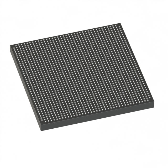
5SGTMC5K3F40I3
| Part Description |
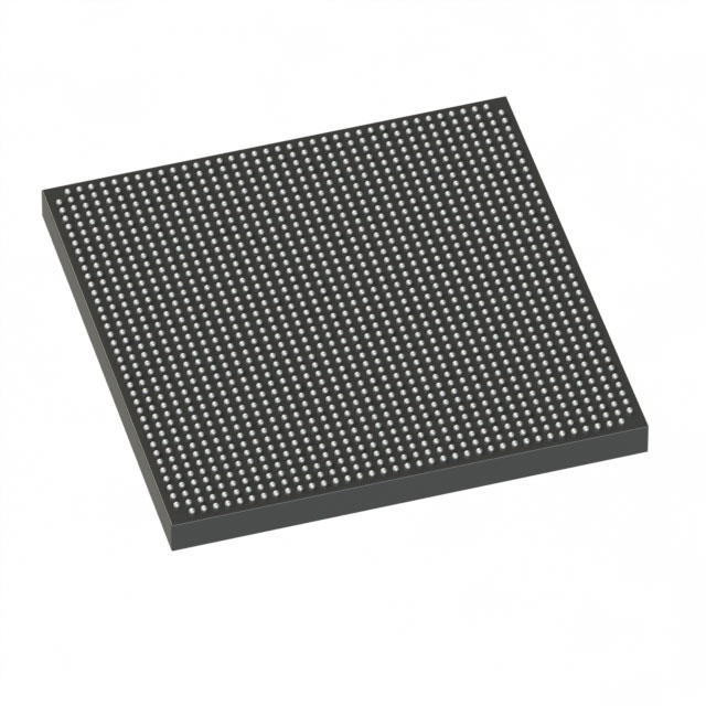
Stratix® V GT Field Programmable Gate Array (FPGA) IC 600 46080000 425000 1517-BBGA, FCBGA |
|---|---|
| Quantity | 279 Available (as of October 7, 2026) |
| Product Category | Field Programmable Gate Array (FPGA) |
|---|---|
| Manufacturer | Intel |
| Manufacturing Status | Obsolete |
| Manufacturer Standard Lead Time | Contact Us |
| Datasheet |
Specifications & Environmental
| Device Package | 1517-FBGA (40x40) | Grade | Industrial | Operating Temperature | -40°C – 100°C | ||
|---|---|---|---|---|---|---|---|
| Package / Case | 1517-BBGA, FCBGA | Number of I/O | 600 | Voltage | 820 mV - 880 mV | ||
| Mounting Method | Surface Mount | RoHS Compliance | Unknown | REACH Compliance | REACH Unknown | ||
| Moisture Sensitivity Level | 3 (168 Hours) | Number of LABs/CLBs | 160500 | Number of Logic Elements/Cells | 425000 | ||
| Number of Gates | N/A | ECCN | OBSOLETE | HTS Code | 0000.00.0000 | ||
| Qualification | N/A | Total RAM Bits | 46080000 |
Overview of 5SGTMC5K3F40I3 – Stratix® V GT FPGA, 425,000 logic elements, 600 I/Os
The 5SGTMC5K3F40I3 is a high-capacity Field Programmable Gate Array (FPGA) designed for industrial applications. It combines large programmable fabric, abundant on-chip memory, and a rich set of clock and DSP resources to support complex digital designs and system integration.
Key architectural highlights include 425,000 logic elements, approximately 46 Mbits of embedded memory, and up to 600 general-purpose I/O pins in a 1517-BBGA FCBGA package. The device operates over an industrial temperature range and supports low-voltage core supply to align with modern system power budgets.
Key Features
- Logic Capacity 425,000 logic elements and 641,600 registers provide substantial programmable resources for sizeable logic and control functions.
- Embedded Memory Approximately 46 Mbits of on-chip RAM for buffering, lookup tables, and state retention within the FPGA fabric.
- DSP Resources 256 dedicated 18×18 multipliers to accelerate arithmetic, filtering, and signal-processing tasks.
- Clocking and Timing 16 global clocks, 92 regional clocks and 28 PLLs enable flexible clock-domain partitioning and precise timing control across large designs.
- I/O and SerDes-Friendly I/O Up to 600 GPIOs and support for up to 150 LVDS channels provide high-density interfacing options for parallel and differential signaling.
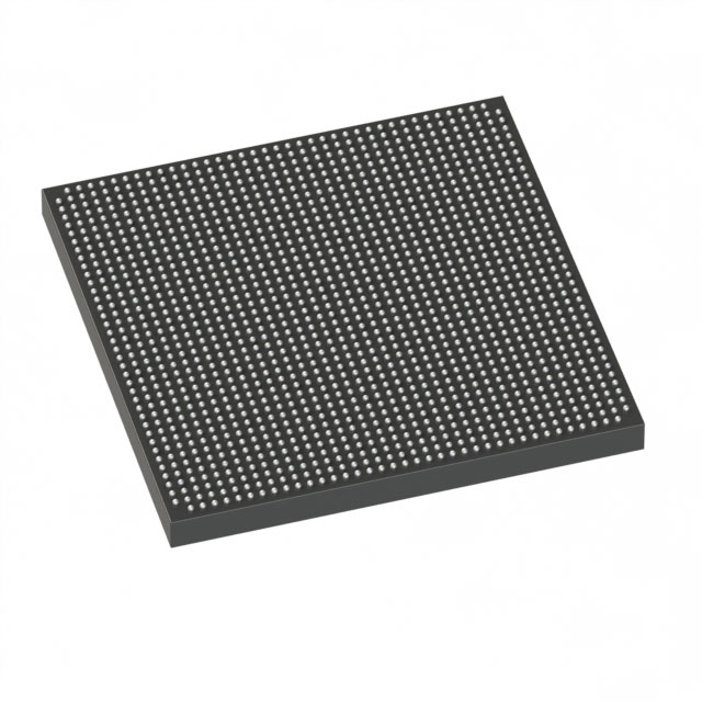
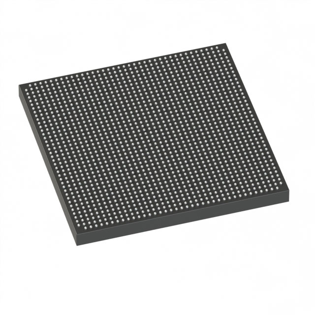
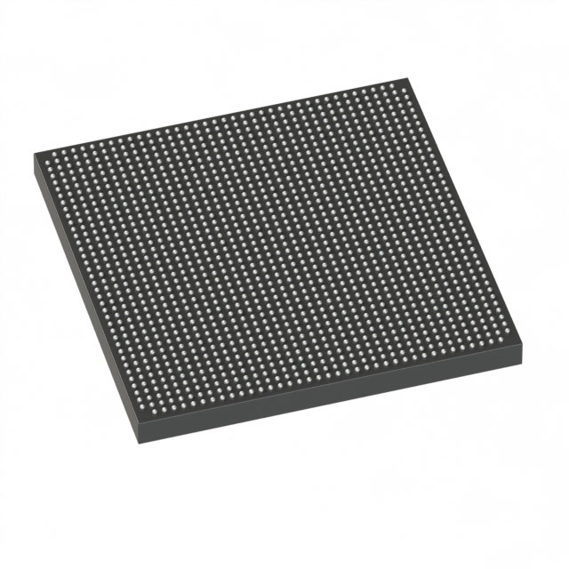
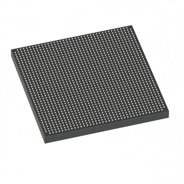
- Package and Mounting Supplied in a 1517-BBGA (1517-FBGA, 40×40) FCBGA package for compact, high-pin-count surface-mount integration.
- Power and Temperature Core voltage range of 820 mV to 880 mV and industrial operating temperature from −40 °C to 100 °C for robust operation in demanding environments.
- Compliance RoHS compliant for regulatory and environmental considerations.
Unique Advantages
- High logic density: 425,000 logic elements enable consolidation of complex functions onto a single device, reducing board-level component count.
- Significant on-chip memory: Approximately 46 Mbits of embedded RAM supports data buffering and stateful processing without immediate reliance on external memory.
- Strong DSP capability: 256 18×18 multipliers accelerate compute-intensive workloads such as filtering, transforms, and fixed-point math.
- Flexible clock infrastructure: Multiple global and regional clocks plus 28 PLLs simplify multi-domain timing and clock distribution for large designs.
- High I/O density: Up to 600 GPIOs and 150 LVDS channels offer extensive external interfacing for sensors, peripherals, and high-speed differential links.
- Industrial-grade robustness: Wide operating temperature range (−40 °C to 100 °C) and RoHS compliance support deployment in industrial environments.
Why Choose 5SGTMC5K3F40I3?
The 5SGTMC5K3F40I3 positions itself for designs that require substantial programmable logic, embedded memory, and DSP acceleration in an industrial-grade FPGA. Its combination of high logic element count, dedicated multipliers, abundant clocking resources, and extensive I/O density makes it suitable for complex system integration where on-chip capacity and reliability matter.
This part is suited to engineering teams and procurement looking for a scalable, RoHS-compliant FPGA solution with a surface-mount FCBGA footprint and operating characteristics tailored to industrial applications. The device’s resource balance supports consolidation of multiple functions onto a single silicon platform, helping simplify BOM and board-level design.
Request a quote or submit an inquiry to receive pricing, lead-time, and availability information for part number 5SGTMC5K3F40I3.





















Date Founded: 1968
Headquarters: Santa Clara, California, USA
Employees: 130,000+
Revenue: $54.23 Billion
Certifications and Memberships: ISO9001:2015, ISO14001:2015, ISO17025:2017, ISO27001:2022, ISO45001:2018, ISO50001:2018


