
5SGTMC7K3F40C2
| Part Description |
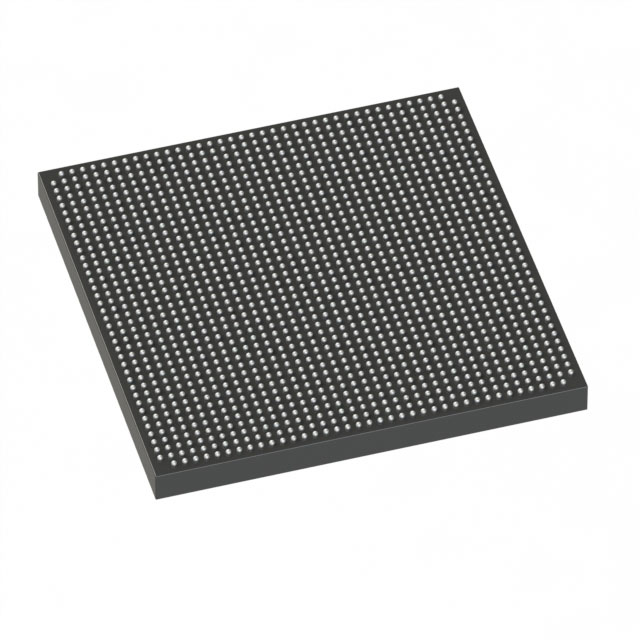
Stratix® V GT Field Programmable Gate Array (FPGA) IC 600 51200000 622000 1517-BBGA, FCBGA |
|---|---|
| Quantity | 238 Available (as of June 15, 2026) |

| Product Category | Field Programmable Gate Array (FPGA) |
|---|---|
| Manufacturer | Intel |
| Manufacturing Status | Obsolete |
| Manufacturer Standard Lead Time | Contact Us |
| Datasheet |
Specifications & Environmental
| Device Package | 1517-FBGA (40x40) | Grade | Commercial | Operating Temperature | 0°C – 85°C | ||
|---|---|---|---|---|---|---|---|
| Package / Case | 1517-BBGA, FCBGA | Number of I/O | 600 | Voltage | 870 mV - 930 mV | ||
| Mounting Method | Surface Mount | RoHS Compliance | Unknown | REACH Compliance | REACH Unknown | ||
| Moisture Sensitivity Level | 3 (168 Hours) | Number of LABs/CLBs | 234750 | Number of Logic Elements/Cells | 622000 | ||
| Number of Gates | N/A | ECCN | OBSOLETE | HTS Code | 0000.00.0000 | ||
| Qualification | N/A | Total RAM Bits | 51200000 |
Overview of 5SGTMC7K3F40C2 – Stratix® V GT FPGA, 622,000 logic elements
The 5SGTMC7K3F40C2 is a Stratix® V GT Field Programmable Gate Array (FPGA) supplied in a 1517-BBGA FCBGA package for surface-mount applications. It provides a high logic density device architecture with 622,000 logic elements and abundant I/O, targeted at FPGA-based system designs that require large on-chip memory and extensive programmable logic resources.
Key value propositions include high logic capacity, substantial embedded memory (approximately 51.2 Mbits), and a broad set of clocking resources and DSP primitives suitable for complex, performance-oriented FPGA implementations within commercial temperature ranges.
Key Features
- Logic Capacity — 622,000 logic elements (cells) and 234,750 CLBs/LABs equivalent indicate substantial programmable logic for large designs.
- Embedded Memory — Approximately 51.2 Mbits of on-chip RAM to support large buffers, FIFOs, and memory-mapped logic functions.
- Registers and DSP Resources — Series datasheet lists 938,880 registers and DSP resources including 256 18×18 multipliers plus 256 hardened single-precision floating-point multipliers/adders for intensive arithmetic and signal-processing tasks.
- I/O and Signaling — 600 general-purpose I/Os (GPIOs) on this part with series-level support up to 776 user I/O pins and up to 150 LVDS channels for high-channel-count connectivity.
- Clocking and PLLs — 16 global clocks, 92 regional clocks, and 28 PLLs as documented in the series-level datasheet provide flexible clock distribution and low-jitter clocking options.
- Package & Mounting — 1517-BBGA (1517-FBGA, 40×40) FCBGA package, surface-mount mounting for dense PCB implementations.
- Power & Operating Range — Core voltage supply range of 870 mV to 930 mV; commercial operating temperature range from 0 °C to 85 °C.
- Compliance — RoHS compliant, meeting common environmental requirements for electronic assemblies.
Typical Applications
- High-density logic and system prototyping — Large logic element count and substantial on-chip RAM support complex prototypes and system-on-chip implementations.
- Multi-channel I/O systems — Hundreds of GPIOs and series-level LVDS channel support enable designs requiring high parallel I/O bandwidth and channel count.
- Signal processing and arithmetic acceleration — Integrated multipliers and hardened floating-point units provide resources for computation-heavy processing pipelines.
Unique Advantages
- High logic integration: 622,000 logic elements allow consolidation of large design functions into a single FPGA, reducing BOM and board complexity.
- Substantial embedded memory: Approximately 51.2 Mbits of on-chip RAM supports deep buffering and memory-intensive algorithms without external memory dependency.
- Rich clocking fabric: Multiple global and regional clocks plus 28 PLLs support complex timing domains and flexible clock architecture.
- Dedicated DSP resources: Numerous multipliers and floating-point units accelerate fixed- and floating-point computation blocks directly in fabric.
- Commercial temperature and RoHS compliance: Designed for commercial applications with RoHS-conformant materials for regulatory compliance in many assemblies.
Why Choose 5SGTMC7K3F40C2?
The 5SGTMC7K3F40C2 positions itself as a high-capacity, commercially graded Stratix® FPGA option for designers needing substantial programmable logic, embedded memory, and DSP resources in a single package. Its combination of hundreds of I/O, extensive clocking resources, and hardened arithmetic blocks make it suitable for complex digital systems that prioritize on-chip integration and scalable performance.
For teams focused on board-level density and long-term design scalability, this device offers capabilities to reduce external component count and consolidate functionality, backed by series-level datasheet specifications for clocking, I/O, and DSP primitives.
Request a quote or submit an inquiry to receive pricing and availability information for 5SGTMC7K3F40C2 and support for volume purchasing or design-in assistance.


Date Founded: 1968
Headquarters: Santa Clara, California, USA
Employees: 130,000+
Revenue: $54.23 Billion
Certifications and Memberships: ISO9001:2015, ISO14001:2015, ISO17025:2017, ISO27001:2022, ISO45001:2018, ISO50001:2018


