
5SGXEA4K1F40C2N
| Part Description |
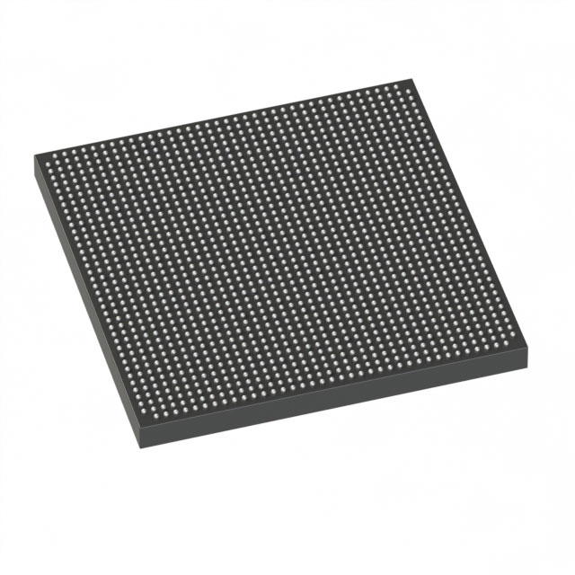
Stratix® V GX Field Programmable Gate Array (FPGA) IC 696 37888000 420000 1517-BBGA, FCBGA |
|---|---|
| Quantity | 659 Available (as of June 10, 2026) |

| Product Category | Field Programmable Gate Array (FPGA) |
|---|---|
| Manufacturer | Intel |
| Manufacturing Status | Obsolete |
| Manufacturer Standard Lead Time | Contact Us |
| Datasheet |
Specifications & Environmental
| Device Package | 1517-FBGA (40x40) | Grade | Commercial | Operating Temperature | 0°C – 85°C | ||
|---|---|---|---|---|---|---|---|
| Package / Case | 1517-BBGA, FCBGA | Number of I/O | 696 | Voltage | 870 mV - 930 mV | ||
| Mounting Method | Surface Mount | RoHS Compliance | RoHS Compliant | REACH Compliance | REACH Unknown | ||
| Moisture Sensitivity Level | 3 (168 Hours) | Number of LABs/CLBs | 158500 | Number of Logic Elements/Cells | 420000 | ||
| Number of Gates | N/A | ECCN | 3A001A2C | HTS Code | 8542.39.0001 | ||
| Qualification | N/A | Total RAM Bits | 37888000 |
Overview of 5SGXEA4K1F40C2N – Stratix® V GX Field Programmable Gate Array (FPGA)
The 5SGXEA4K1F40C2N is a Stratix® V GX family FPGA from Intel, delivered in a 1517-BBGA FCBGA package. It provides very large programmable logic capacity and on-chip memory combined with a high I/O count, all in a surface-mount package rated for commercial temperature operation.
This device is suitable for designs that require extensive logic resources, substantial embedded RAM, and many external interfaces, with explicit electrical and mechanical specifications for integration and power budgeting.
Key Features
- Logic Capacity Approximately 420,000 logic elements for complex digital designs; device data also lists 158,500 LABs.
- Embedded Memory Approximately 37.9 Mbits of on-chip RAM to support large buffering, tables, and state storage.
- I/O Up to 696 user I/O pins, enabling high channel counts and extensive external device connectivity.
- Package & Mounting 1517-BBGA, FCBGA package (supplier device package: 1517-FBGA, 40×40) with surface-mount mounting for compact PCB integration.
- Power Core voltage supply range of 870 mV to 930 mV for power planning and supply design.
- Temperature & Grade Commercial grade with an operating temperature range of 0 °C to 85 °C.
- Compliance RoHS compliant.
- Manufacturer Intel Stratix V GX device family (device datasheet and technical documentation available from the manufacturer).
Typical Applications
- High-density digital processing Leverage ~420,000 logic elements and large embedded RAM to implement complex algorithms and parallel data paths directly in programmable logic.
- Multi-channel interfacing The 696 I/O pins support designs requiring many simultaneous external interfaces, board-level hubs, or large sensor arrays.
- Buffering and packet handling Approximately 37.9 Mbits of on-chip memory provides capacity for buffering, packet queues, and lookup tables in communication or data-acquisition systems.
Unique Advantages
- Massive logic resources: The large logic element count enables consolidation of complex subsystems into a single FPGA, reducing BOM and board area.
- Substantial embedded memory: Nearly 38 Mbits of on-chip RAM reduces dependence on external memory for many buffering and caching needs.
- Extensive external connectivity: 696 I/O pins let you interface to many peripherals and high-channel-count front-ends without adding extra devices.
- Compact, manufacturable package: The 1517-BBGA (1517-FBGA, 40×40) surface-mount package balances high pin count with a board-friendly form factor.
- Clear electrical parameters: Defined core supply range (870–930 mV) simplifies power-supply design and validation.
- Commercial temperature coverage: Rated 0 °C to 85 °C for standard commercial deployments and controlled-environment systems.
Why Choose 5SGXEA4K1F40C2N?
The 5SGXEA4K1F40C2N combines a very high logic element count, substantial embedded RAM, and a large I/O complement in a manufacturable FCBGA package, making it a strategic choice for designs that require integration of complex digital functions and extensive external connectivity. As a member of the Stratix V GX family from Intel, the device is backed by family-level documentation and electrical characteristics to support system integration and power budgeting.
This part is ideal for engineering teams building high-capacity FPGA-based systems that demand on-chip memory and numerous interfaces while working within commercial temperature ranges and standard surface-mount assembly processes.
Request a quote or submit an inquiry to obtain pricing and availability for the 5SGXEA4K1F40C2N and to discuss lead times or volume purchasing options.


Date Founded: 1968
Headquarters: Santa Clara, California, USA
Employees: 130,000+
Revenue: $54.23 Billion
Certifications and Memberships: ISO9001:2015, ISO14001:2015, ISO17025:2017, ISO27001:2022, ISO45001:2018, ISO50001:2018


