
5SGXEA5K2F40I3LN
| Part Description |
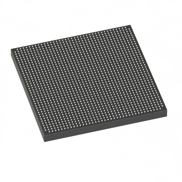
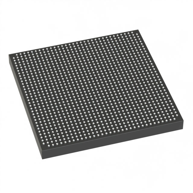
Stratix® V GX Field Programmable Gate Array (FPGA) IC 696 46080000 490000 1517-BBGA, FCBGA |
|---|---|
| Quantity | 499 Available (as of June 15, 2026) |

| Product Category | Field Programmable Gate Array (FPGA) |
|---|---|
| Manufacturer | Intel |
| Manufacturing Status | Obsolete |
| Manufacturer Standard Lead Time | Contact Us |
| Datasheet |
Specifications & Environmental
| Device Package | 1517-FBGA (40x40) | Grade | Industrial | Operating Temperature | -40°C – 100°C | ||
|---|---|---|---|---|---|---|---|
| Package / Case | 1517-BBGA, FCBGA | Number of I/O | 696 | Voltage | 820 mV - 880 mV | ||
| Mounting Method | Surface Mount | RoHS Compliance | RoHS Compliant | REACH Compliance | REACH Unknown | ||
| Moisture Sensitivity Level | 3 (168 Hours) | Number of LABs/CLBs | 185000 | Number of Logic Elements/Cells | 490000 | ||
| Number of Gates | N/A | ECCN | 3A001A2C | HTS Code | 8542.39.0001 | ||
| Qualification | N/A | Total RAM Bits | 46080000 |
Overview of 5SGXEA5K2F40I3LN – Stratix® V GX Field Programmable Gate Array (FPGA)
The 5SGXEA5K2F40I3LN is a Stratix® V GX family FPGA IC from Intel, offering very high logic density and extensive I/O for demanding programmable-logic designs. It integrates approximately 490,000 logic elements and approximately 46.08 Mbits of embedded memory, making it suitable for high-channel-count and high-bandwidth applications that require large on-chip resources and flexible I/O.
Packaged in a 1517-ball FCBGA (1517-FBGA, 40×40) with surface-mount mounting and rated for industrial temperatures, this device is specified for a core voltage supply range of 820 mV to 880 mV and an operating temperature range of −40 °C to 100 °C.
Key Features
- High Logic Density — Approximately 490,000 logic elements and 185,000 logic blocks provide large programmable fabric for complex algorithms and multi-function designs.
- Embedded Memory — Approximately 46.08 Mbits of on-chip RAM to support large buffers, lookup tables, and state storage without external memory.
- Extensive I/O — Up to 696 user I/Os to interface with multiple high-pin-count peripherals, parallel buses, and multi-lane interfaces.
- Transceiver Capability (Series) — Stratix V GX devices include transceiver speed grades documented up to 14.1 Gbps (series-level specification), enabling high-speed serial link designs when using the appropriate transceiver grade.
- Power and Core Supply — Core voltage supply specified from 820 mV to 880 mV for predictable power planning and power-delivery design.
- Industrial Temperature Grade — Specified operating range from −40 °C to 100 °C for deployment in industrial environments.
- Package and Mounting — 1517-BBGA FCBGA package (supplier package: 1517-FBGA, 40×40) with surface-mount mounting for compact PCB integration.
- RoHS Compliant — Meets RoHS requirements for lead-free manufacturing and regulatory compliance.
Typical Applications
- High‑speed communications — Leverage the Stratix V GX transceiver speed grades and large logic/memory resources for packet processing, line cards, and multi-gigabit serial links.
- Networking and data center — Implement complex packet engines, protocol offloads, and high‑density switching functions using the device’s extensive I/O and on‑chip memory.
- Compute acceleration — Deploy as a hardware accelerator for dataflow, DSP, or custom compute pipelines requiring large logic capacity and embedded memory.
- Industrial systems — Use the industrial temperature grade and high I/O count for control systems, test equipment, and instrumentation that require robust operation across −40 °C to 100 °C.
Unique Advantages
- Large programmable fabric: Enables consolidation of multiple subsystems into a single FPGA, reducing board-level complexity and BOM.
- Substantial on-chip RAM: Approximately 46.08 Mbits of embedded memory reduces reliance on external memory and improves data locality and throughput.
- High I/O count: 696 user I/Os simplify interfacing to multi-channel front ends, wide parallel buses, and dense connector systems.
- Industrial temperature rating: Operation from −40 °C to 100 °C supports deployment in harsher environments without additional qualification statements.
- Well-defined power window: Core supply range of 820 mV–880 mV assists predictable power-supply design and thermal planning.
- RoHS compliance: Facilitates integration into modern, lead‑free production flows.
Why Choose 5SGXEA5K2F40I3LN?
The 5SGXEA5K2F40I3LN places a large Stratix V GX FPGA fabric, substantial embedded memory, and a very high I/O count into a compact 1517‑ball FCBGA package rated for industrial temperatures. It is suited for system designs that require high logic capacity, extensive connectivity, and on‑chip memory to implement complex, high-throughput functions while maintaining predictable power and thermal parameters.
Its specification makes it a practical choice for engineering teams building high-speed communications systems, networking equipment, compute accelerators, and industrial platforms that require scalable programmable logic and a robust component footprint from a recognized FPGA family.
Request a quote or submit an inquiry to receive pricing and availability information for the 5SGXEA5K2F40I3LN.


Date Founded: 1968
Headquarters: Santa Clara, California, USA
Employees: 130,000+
Revenue: $54.23 Billion
Certifications and Memberships: ISO9001:2015, ISO14001:2015, ISO17025:2017, ISO27001:2022, ISO45001:2018, ISO50001:2018


