
5SGXEB5R1F43C2L
| Part Description |
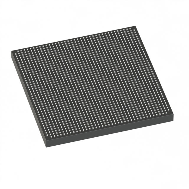
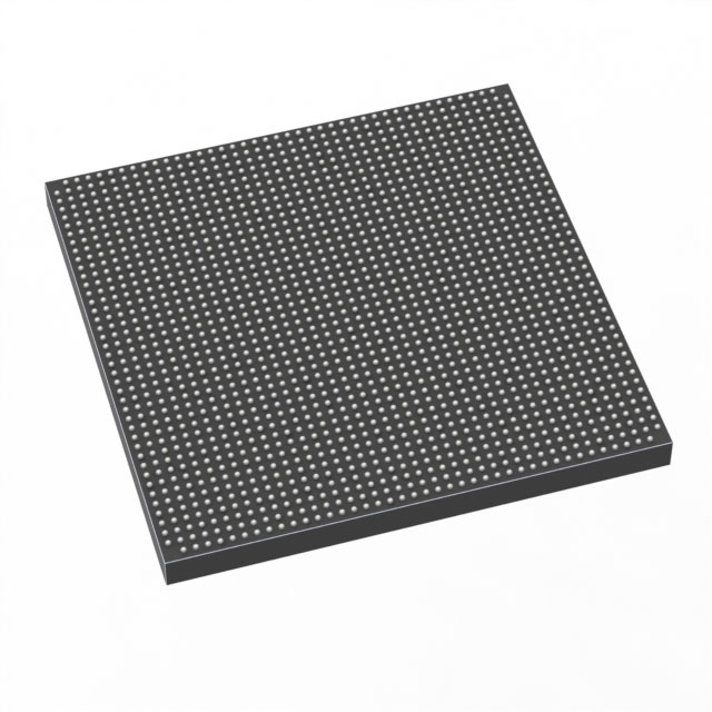
Stratix® V GX Field Programmable Gate Array (FPGA) IC 600 41984000 490000 1760-BBGA, FCBGA |
|---|---|
| Quantity | 1,363 Available (as of June 15, 2026) |

| Product Category | Field Programmable Gate Array (FPGA) |
|---|---|
| Manufacturer | Intel |
| Manufacturing Status | Obsolete |
| Manufacturer Standard Lead Time | Contact Us |
| Datasheet |
Specifications & Environmental
| Device Package | 1760-FCBGA (42.5x42.5) | Grade | Commercial | Operating Temperature | 0°C – 85°C | ||
|---|---|---|---|---|---|---|---|
| Package / Case | 1760-BBGA, FCBGA | Number of I/O | 600 | Voltage | 820 mV - 880 mV | ||
| Mounting Method | Surface Mount | RoHS Compliance | RoHS Compliant | REACH Compliance | REACH Unknown | ||
| Moisture Sensitivity Level | 3 (168 Hours) | Number of LABs/CLBs | 185000 | Number of Logic Elements/Cells | 490000 | ||
| Number of Gates | N/A | ECCN | 3A001A2C | HTS Code | 8542.39.0001 | ||
| Qualification | N/A | Total RAM Bits | 41984000 |
Overview of 5SGXEB5R1F43C2L – Stratix® V GX FPGA, 1760-FCBGA
The 5SGXEB5R1F43C2L is a Stratix V GX field-programmable gate array (FPGA) in a 1760‑FBGA (1760‑FCBGA, 42.5×42.5 mm) package. It delivers high on-chip logic density and embedded memory for complex, I/O‑heavy designs and is offered in a commercial temperature grade.
Designed for applications that require large programmable logic capacity, abundant I/O and low-voltage core operation, the device combines approximately 490,000 logic elements with roughly 42 Mbits of embedded RAM and support for series-level high-speed transceiver grades described in the Stratix V GX family datasheet.
Key Features
- Logic Capacity — 490,000 logic elements for large, multi‑function FPGA designs and partitioned hardware acceleration.
- Embedded Memory — Approximately 42 Mbits of on‑chip RAM to support buffers, FIFOs and local data storage.
- I/O Density — 600 user I/O pins to enable broad external connectivity and multi‑lane interfaces.
- High‑speed Transceiver Family Support — Stratix V GX series transceiver speed grades are documented in the device family datasheet, including GX channel grades up to the speeds listed for the series.
- Power and Core Supply — Core supply voltage range specified at 820 mV to 880 mV to match low‑voltage power domains.
- Package and Mounting — 1760‑FCBGA surface‑mount package (42.5 × 42.5 mm) for high‑density board implementations.
- Commercial Temperature Grade — Rated for 0 °C to 85 °C operation for standard commercial applications.
- RoHS Compliant — Meets RoHS requirements for lead‑free assembly and environmental compliance.
Typical Applications
- High‑density custom logic — Use the large logic element count and abundant embedded RAM to implement complex custom accelerators and processing pipelines.
- High‑bandwidth I/O systems — The 600 I/O pins and family transceiver capabilities support multi‑lane interfaces and board‑level connectivity tasks.
- Data buffering and packet processing — Substantial on‑chip memory and logic resources facilitate packet buffering, queuing and protocol processing functions.
Unique Advantages
- Extensive programmable logic: 490,000 logic elements simplify integration of multiple functions into a single device, reducing board count and BOM complexity.
- Significant embedded memory: Approximately 42 Mbits of RAM enables local data storage and low‑latency buffering without external memory for many use cases.
- High I/O count: 600 I/O pins offer flexibility for multi‑channel interfaces and dense peripheral connectivity.
- Compact, high‑density package: The 1760‑FCBGA (42.5 × 42.5 mm) package supports complex, space‑constrained board designs while maintaining surface‑mount compatibility.
- Low‑voltage core operation: Specified core supply range of 820–880 mV aligns with low‑power core domains and modern power architectures.
- Commercial grade reliability: Rated for 0 °C to 85 °C operation and RoHS compliant for standard commercial deployments.
Why Choose 5SGXEB5R1F43C2L?
The 5SGXEB5R1F43C2L positions itself where high programmable density, substantial embedded memory and broad I/O capability are required in commercial‑grade systems. Its Stratix V GX family heritage provides documented transceiver and I/O performance characteristics at the series level, while the part’s package and power specifications make it suitable for compact board layouts with low‑voltage core rails.
Choose this FPGA for complex system designs that benefit from consolidating logic, memory and high‑pin‑count interfaces into a single, RoHS‑compliant component backed by the Stratix V device documentation and design ecosystem.
Request a quote or contact sales to get pricing, availability and technical support for the 5SGXEB5R1F43C2L.


Date Founded: 1968
Headquarters: Santa Clara, California, USA
Employees: 130,000+
Revenue: $54.23 Billion
Certifications and Memberships: ISO9001:2015, ISO14001:2015, ISO17025:2017, ISO27001:2022, ISO45001:2018, ISO50001:2018


