
5SGXMA5K2F40C2G
| Part Description |
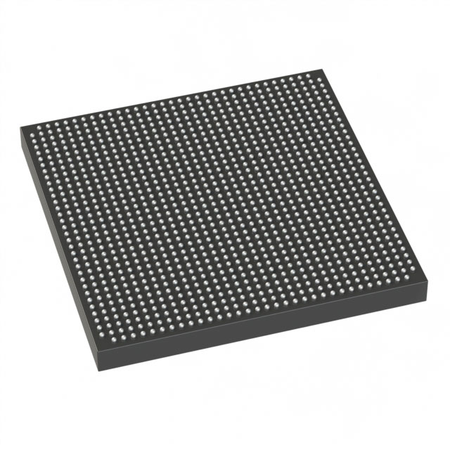
Stratix® V GX Field Programmable Gate Array (FPGA) IC 696 46080000 490000 1517-BBGA, FCBGA |
|---|---|
| Quantity | 1,705 Available (as of June 15, 2026) |

| Product Category | Field Programmable Gate Array (FPGA) |
|---|---|
| Manufacturer | Intel |
| Manufacturing Status | Active |
| Manufacturer Standard Lead Time | 26 Weeks |
| Datasheet |
Specifications & Environmental
| Device Package | 1517-FBGA (40x40) | Grade | Commercial | Operating Temperature | 0°C – 85°C | ||
|---|---|---|---|---|---|---|---|
| Package / Case | 1517-BBGA, FCBGA | Number of I/O | 696 | Voltage | 870 mV - 930 mV | ||
| Mounting Method | Surface Mount | RoHS Compliance | RoHS Compliant | REACH Compliance | REACH Unaffected | ||
| Moisture Sensitivity Level | 3 (168 Hours) | Number of LABs/CLBs | 185000 | Number of Logic Elements/Cells | 490000 | ||
| Number of Gates | N/A | ECCN | N/A | HTS Code | N/A | ||
| Qualification | N/A | Total RAM Bits | 46080000 |
Overview of 5SGXMA5K2F40C2G – Stratix® V GX Field Programmable Gate Array (FPGA) IC 490,000 logic elements, ~46 Mbits RAM, 696 I/Os
The 5SGXMA5K2F40C2G is a Stratix® V GX family FPGA from Intel, delivering high logic density and substantial embedded RAM in a high-pin-count FCBGA package. It is designed for complex programmable logic implementations that require a large number of logic elements, extensive I/O, and support for the Stratix V GX device series electrical and transceiver characteristics documented in the device datasheet.
As a commercial-grade device, this FPGA targets designs that demand high integration, flexible I/O, and significant on-chip memory while operating within standard commercial temperature and supply conditions.
Key Features
- Core capacity — 490,000 logic elements for large-scale combinational and sequential logic integration.
- Embedded memory — approximately 46 Mbits of on-chip RAM to support buffering, FIFOs, and memory-intensive algorithms.
- I/O — 696 user I/Os to support dense pinout requirements and multiple parallel interfaces.
- Transceiver family (Stratix V GX) — device belongs to the Stratix V GX family with documented transceiver speed grades in the Stratix V device datasheet.
- Power supply — core voltage operating range from 870 mV to 930 mV for system power budgeting and regulator selection.
- Package & mounting — 1517-BBGA (FCBGA) supplier package 1517-FBGA (40×40) in a surface-mount format for high-density board designs.
- Commercial grade temperature — rated for 0°C to 85°C operating temperature.
- RoHS compliant — conforms to lead-free manufacturing and environmental requirements.
Typical Applications
- High-density digital processing — large logic capacity and embedded RAM support complex signal processing, custom compute, and algorithm acceleration implementations.
- Communications and high-speed data transport — Stratix V GX family transceiver capability and large I/O count make the device suited for networking, backplane, and multi-gigabit interface designs as described in the device documentation.
- Prototyping and system integration — ample logic resources and on-chip memory enable integration of multiple subsystems and rapid hardware prototyping.
Unique Advantages
- High logic capacity: 490,000 logic elements provide the headroom to implement large, complex designs without external glue logic.
- Substantial on-chip memory: approximately 46 Mbits of embedded RAM reduces reliance on external memory for buffering and intermediate storage.
- Extensive I/O availability: 696 I/Os accommodate dense peripheral connectivity and parallel interfaces.
- Compact, high-density packaging: 1517-BBGA (FCBGA) surface-mount package enables a high pin-count solution in a space-efficient footprint.
- Commercial temperature and supply ranges: defined 0°C–85°C operating range and 870 mV–930 mV core supply simplify system-level thermal and power planning.
- RoHS compliant: meets environmental requirements for lead-free assembly processes.
Why Choose 5SGXMA5K2F40C2G?
The 5SGXMA5K2F40C2G delivers a combination of large-scale programmable logic, significant embedded memory, and extensive I/O in the Stratix V GX device family package. Its commercial-grade ratings and documented electrical and switching characteristics make it suitable for engineering teams building high-density FPGA systems that require predictable operating conditions and integration with the Stratix V ecosystem.
This device is appropriate for designers who need scalable logic resources, on-chip storage, and dense connectivity in a surface-mount FCBGA package, backed by the technical documentation available for the Stratix V family.
Request a quote or submit a sales inquiry to obtain pricing and availability for the 5SGXMA5K2F40C2G and start planning integration into your next high-density FPGA design.


Date Founded: 1968
Headquarters: Santa Clara, California, USA
Employees: 130,000+
Revenue: $54.23 Billion
Certifications and Memberships: ISO9001:2015, ISO14001:2015, ISO17025:2017, ISO27001:2022, ISO45001:2018, ISO50001:2018


