
5SGXMA5N1F40C2LN
| Part Description |
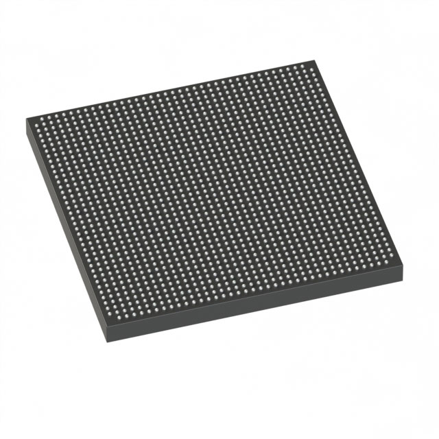
Stratix® V GX Field Programmable Gate Array (FPGA) IC 600 46080000 490000 1517-BBGA, FCBGA |
|---|---|
| Quantity | 393 Available (as of June 14, 2026) |

| Product Category | Field Programmable Gate Array (FPGA) |
|---|---|
| Manufacturer | Intel |
| Manufacturing Status | Obsolete |
| Manufacturer Standard Lead Time | Contact Us |
| Datasheet |
Specifications & Environmental
| Device Package | 1517-FBGA (40x40) | Grade | Commercial | Operating Temperature | 0°C – 85°C | ||
|---|---|---|---|---|---|---|---|
| Package / Case | 1517-BBGA, FCBGA | Number of I/O | 600 | Voltage | 820 mV - 880 mV | ||
| Mounting Method | Surface Mount | RoHS Compliance | RoHS Compliant | REACH Compliance | REACH Unknown | ||
| Moisture Sensitivity Level | 3 (168 Hours) | Number of LABs/CLBs | 185000 | Number of Logic Elements/Cells | 490000 | ||
| Number of Gates | N/A | ECCN | 3A001A2C | HTS Code | 8542.39.0001 | ||
| Qualification | N/A | Total RAM Bits | 46080000 |
Overview of 5SGXMA5N1F40C2LN – Stratix® V GX Field Programmable Gate Array (FPGA)
The 5SGXMA5N1F40C2LN is a Stratix® V GX family Field Programmable Gate Array (FPGA) offered in a 1517-BBGA FCBGA package. It delivers high on-chip logic capacity, substantial embedded memory, and a large I/O count for complex, high-density FPGA designs.
Targeted at commercial applications, this device combines approximately 490,000 logic elements, roughly 46.08 Mbits of embedded memory, and 600 I/O pins to enable dense digital processing, heavy connectivity, and designs that require significant programmable resources.
Key Features
- Logic Capacity Approximately 490,000 logic elements to implement large, complex digital designs and custom hardware accelerators.
- Embedded Memory Approximately 46.08 Mbits of on-chip RAM to support buffering, lookup tables, and memory-intensive algorithms.
- I/O Density 600 available I/O pins for broad external connectivity and multi-channel interfaces.
- Transceiver Family (Series-level) Stratix V GX series transceiver options are documented at the device-family level, including GX channel speeds up to 14.1 Gbps for high-speed serial links.
- Power Supply Core voltage supply range specified at 820 mV to 880 mV to match system power requirements.
- Package & Mounting 1517-BBGA (FCBGA) package; supplier device package listed as 1517-FBGA (40×40). Surface-mount mounting type for standard PCB assembly.
- Commercial Temperature Grade Operational range 0 °C to 85 °C, suitable for commercial-grade environments.
- Regulatory Compliance RoHS compliant.
Typical Applications
- High-density digital processing Use the device’s large logic element count and embedded memory for compute-intensive FPGA functions and custom accelerators.
- Multi-channel I/O systems 600 I/O pins support complex connectivity requirements for board-level aggregation, interface bridging, and sensor/actuator hubs.
- High-speed serial interfaces Stratix V GX series transceiver capabilities (series-level) enable deployment in systems requiring high-speed serial links.
- Embedded system platforms Large on-chip RAM combined with extensive logic resources suits integration of protocol handling, buffering, and control logic in commercial embedded designs.
Unique Advantages
- High integration density: Large logic and memory resources reduce the need for external components and simplify system-level design.
- Extensive connectivity: 600 I/O pins provide flexibility for interfacing multiple peripherals and high-pin-count subsystems.
- Commercial temperature suitability: Rated for 0 °C to 85 °C operation to meet the needs of commercial electronic products.
- Series-level high-speed transceivers: Stratix V GX transceiver options documented for the family support high-bandwidth serial communications at the series level.
- Industry compliance: RoHS compliance supports environmentally conscious product development and manufacturing.
- Standard surface-mount package: 1517-BBGA (1517-FBGA supplier package) in a 40×40 footprint for established PCB assembly processes.
Why Choose 5SGXMA5N1F40C2LN?
The 5SGXMA5N1F40C2LN positions itself as a high-capacity commercial FPGA for designs that demand substantial programmable logic, significant embedded memory, and broad I/O connectivity. Its Stratix V GX family attributes and series-level transceiver options make it suitable for complex digital systems and high-throughput applications.
Engineers and procurement teams looking for a commercially graded FPGA with integrated resources for dense logic implementation, large on-chip RAM, and extensive external interfacing will find this device aligns with scalable, robust designs while meeting RoHS requirements.
Please request a quote or submit an inquiry to receive pricing, availability, and technical support information for 5SGXMA5N1F40C2LN.


Date Founded: 1968
Headquarters: Santa Clara, California, USA
Employees: 130,000+
Revenue: $54.23 Billion
Certifications and Memberships: ISO9001:2015, ISO14001:2015, ISO17025:2017, ISO27001:2022, ISO45001:2018, ISO50001:2018


