
5SGXMA5N1F40C1N
| Part Description |
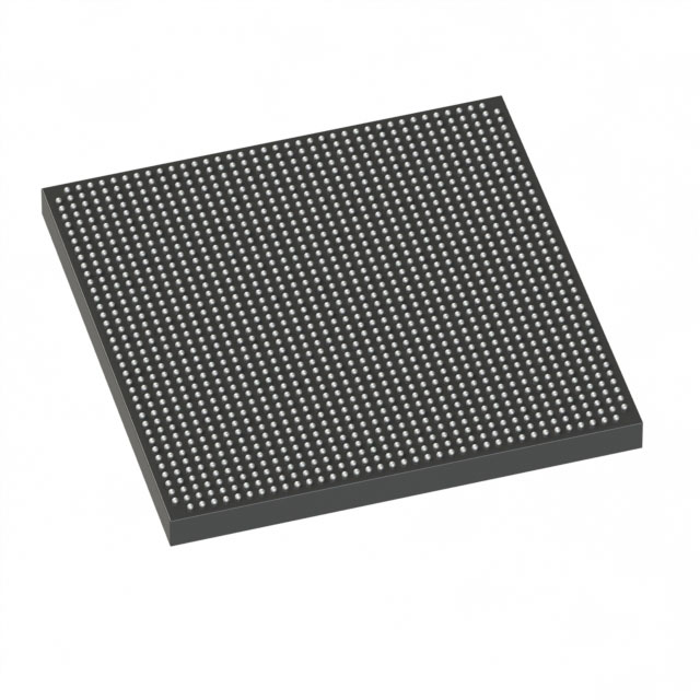
Stratix® V GX Field Programmable Gate Array (FPGA) IC 600 46080000 490000 1517-BBGA, FCBGA |
|---|---|
| Quantity | 318 Available (as of June 15, 2026) |

| Product Category | Field Programmable Gate Array (FPGA) |
|---|---|
| Manufacturer | Intel |
| Manufacturing Status | Obsolete |
| Manufacturer Standard Lead Time | Contact Us |
| Datasheet |
Specifications & Environmental
| Device Package | 1517-FBGA (40x40) | Grade | Commercial | Operating Temperature | 0°C – 85°C | ||
|---|---|---|---|---|---|---|---|
| Package / Case | 1517-BBGA, FCBGA | Number of I/O | 600 | Voltage | 870 mV - 930 mV | ||
| Mounting Method | Surface Mount | RoHS Compliance | RoHS Compliant | REACH Compliance | REACH Unknown | ||
| Moisture Sensitivity Level | 3 (168 Hours) | Number of LABs/CLBs | 185000 | Number of Logic Elements/Cells | 490000 | ||
| Number of Gates | N/A | ECCN | 3A001A2C | HTS Code | 8542.39.0001 | ||
| Qualification | N/A | Total RAM Bits | 46080000 |
Overview of 5SGXMA5N1F40C1N – Stratix® V GX FPGA, approximately 490,000 logic elements, 600 I/Os
The 5SGXMA5N1F40C1N is a Stratix® V GX Field Programmable Gate Array (FPGA) IC from Intel, provided in a 1517-BBGA (FCBGA) package. It delivers a high-density programmable fabric with large embedded memory and extensive I/O capability, suitable for complex digital designs that require substantial logic, memory, and connectivity.
Key value propositions include a high logic element count, approximately 46 Mbits of on-chip RAM, 600 I/O pins, and low-voltage core operation — enabling dense integration of custom logic and high-bandwidth interfacing in commercial-temperature systems.
Key Features
- Core Logic Approximately 490,000 logic elements for implementing large-scale FPGA designs and complex custom logic functions.
- Embedded Memory Approximately 46 Mbits of on-chip RAM to support data buffering, packet processing, and state storage inside the FPGA fabric.
- I/O Capacity 600 I/O pins provide broad connectivity options for multi-channel interfaces and parallel bus architectures.
- Package & Mounting 1517-BBGA (FCBGA) supplier device package listed as 1517-FBGA (40×40); surface-mount device suitable for compact board designs.
- Power & Core Voltage Core operating voltage specified between 870 mV and 930 mV, enabling low-voltage core operation.
- Operating Grade & Temperature Commercial grade device with an operating temperature range of 0 °C to 85 °C.
- Environmental Compliance RoHS compliant.
Typical Applications
- High-performance digital systems Use the large logic fabric and on-chip RAM to implement custom accelerators and complex state machines.
- Multi-channel I/O and interface bridging 600 I/Os enable dense peripheral interfacing, protocol bridging, and parallel processing front-ends.
- Network and packet processing Large embedded memory and logic resources support buffering, parsing, and custom packet-handling pipelines.
- Prototyping and system integration High-density FPGA fabric facilitates system-level prototyping and integration of custom IP blocks.
Unique Advantages
- Highly integrated programmable fabric: Approximately 490,000 logic elements let you consolidate complex logic into a single device, reducing board-level component count.
- Substantial on-chip memory: Approximately 46 Mbits of embedded RAM supports data-intensive tasks without external memory in many use cases.
- Extensive I/O capability: 600 I/O pins provide flexibility for multi-lane interfaces and parallel connectivity.
- Compact FCBGA packaging: 1517-BBGA / 1517-FBGA (40×40) package supports high-density PCB layouts for space-constrained systems.
- Low-voltage core operation: 870 mV to 930 mV core voltage supports modern low-voltage power architectures.
- Commercial temperature range: Rated for 0 °C to 85 °C operation, appropriate for a wide range of commercial applications.
Why Choose 5SGXMA5N1F40C1N?
The 5SGXMA5N1F40C1N positions itself as a high-density, high-connectivity FPGA solution for commercial designs that require substantial programmable logic, embedded memory, and large I/O capacity. Its combination of approximately 490,000 logic elements, roughly 46 Mbits of on-chip RAM, and 600 I/Os enables consolidation of complex digital functions and flexible system interfacing within a single FCBGA package.
This device is well-suited to engineering teams building advanced digital systems, network and packet-processing modules, or integration-heavy prototypes that benefit from a dense FPGA fabric, compact packaging, and low-voltage core operation. RoHS compliance and commercial temperature rating support mainstream product development and deployment.
Request a quote or submit your specifications to get pricing and availability for the 5SGXMA5N1F40C1N. Our team can provide lead-time details and ordering assistance for your project.


Date Founded: 1968
Headquarters: Santa Clara, California, USA
Employees: 130,000+
Revenue: $54.23 Billion
Certifications and Memberships: ISO9001:2015, ISO14001:2015, ISO17025:2017, ISO27001:2022, ISO45001:2018, ISO50001:2018


