
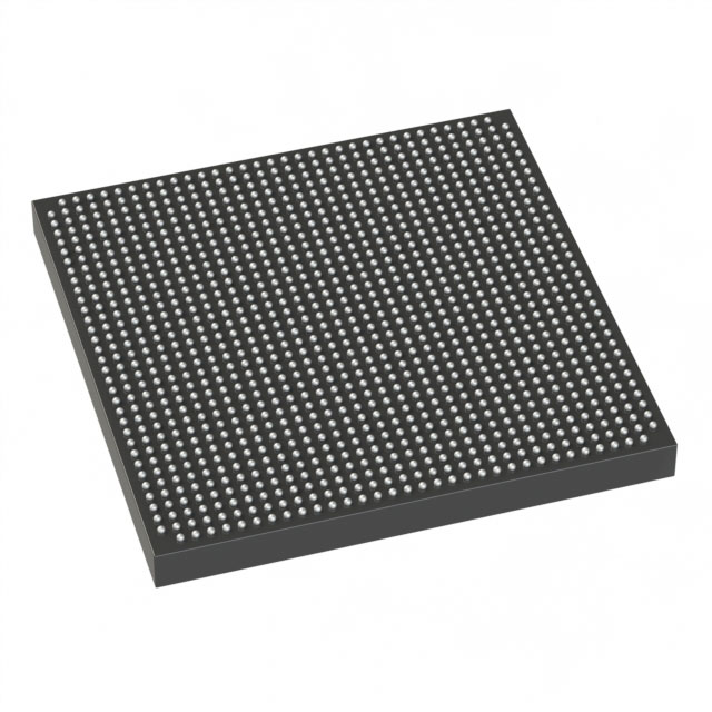
5SGXMA7K2F40C1WN
| Part Description |
Stratix® V GX Field Programmable Gate Array (FPGA) IC 696 51200000 622000 1517-BBGA, FCBGA |
|---|---|
| Quantity | 423 Available (as of June 15, 2026) |

| Product Category | Field Programmable Gate Array (FPGA) |
|---|---|
| Manufacturer | Intel |
| Manufacturing Status | Obsolete |
| Manufacturer Standard Lead Time | Contact Us |
| Datasheet |
Specifications & Environmental
| Device Package | 1517-FBGA (40x40) | Grade | Commercial | Operating Temperature | 0°C – 85°C | ||
|---|---|---|---|---|---|---|---|
| Package / Case | 1517-BBGA, FCBGA | Number of I/O | 696 | Voltage | 870 mV - 930 mV | ||
| Mounting Method | Surface Mount | RoHS Compliance | RoHS non-compliant | REACH Compliance | REACH Unknown | ||
| Moisture Sensitivity Level | 4 (72 Hours) | Number of LABs/CLBs | 234720 | Number of Logic Elements/Cells | 622000 | ||
| Number of Gates | N/A | ECCN | OBSOLETE | HTS Code | N/A | ||
| Qualification | N/A | Total RAM Bits | 51200000 |
Overview of 5SGXMA7K2F40C1WN – Stratix® V GX FPGA, 696 I/Os, 622,000 Logic Elements, 1517-BBGA
The 5SGXMA7K2F40C1WN is a Stratix® V GX Field Programmable Gate Array (FPGA) from Intel, delivered in a 1517-ball FCBGA package for surface-mount assembly. It provides a high logic capacity and large embedded memory, combined with a substantial I/O count for complex, I/O‑intensive designs.
This commercial-grade device targets applications that require extensive programmable logic, abundant on-chip RAM, and a high number of I/Os, while operating within a standard commercial temperature range.
Key Features
- Core Logic Capacity – 622,000 logic elements and 234,720 CLBs provide extensive programmable logic resources for large FPGA designs.
- Embedded Memory – Approximately 51.2 Mbits of on-chip RAM to support buffering, LUTRAM, and memory-intensive functions.
- I/O Density – 696 user I/Os suitable for high-pin-count applications and dense board-level connectivity.
- Transceiver Capability (Series) – Stratix V GX family documentation lists GX transceiver speed grades that can reach up to 14.1 Gbps for appropriate devices in the series.
- Power – Core voltage supply range of 870 mV to 930 mV for core power planning and supply design.
- Package & Mounting – 1517‑BBGA (FCBGA) package, supplier device package 1517‑FBGA (40×40); surface-mount mounting type for standard PCB assembly.
- Commercial Temperature Grade – Rated for 0 °C to 85 °C operation for commercial applications.
- RoHS Compliant – Meets RoHS requirements for lead‑free designs.
Typical Applications
- High-speed serial designs – Use the Stratix V GX family’s transceiver capabilities for designs requiring high-speed serial links and data aggregation.
- Network and communications equipment – Leverage large logic and memory resources alongside high I/O counts for packet processing, protocol implementation, and interface bridging.
- Complex digital processing – Implement compute-heavy FPGA functions such as DSP pipelines, custom accelerators, and wide datapath processing using extensive CLBs and embedded RAM.
Unique Advantages
- High logic scale: 622,000 logic elements and 234,720 CLBs enable large, feature-rich FPGA designs without immediate part migration.
- Substantial on-chip memory: Approximately 51.2 Mbits of embedded RAM reduce reliance on external memory for buffering and state storage.
- Extensive I/O connectivity: 696 I/Os support dense peripheral interfacing and multiple high-pin interfaces on a single device.
- Commercial-ready thermal range: Rated 0 °C to 85 °C to match standard commercial product requirements and testing workflows.
- Package for high-density boards: 1517‑BBGA (40×40 FCBGA) enables compact board layouts while providing large I/O and routing capability.
- Regulatory compliance: RoHS compliance supports lead‑free manufacturing and global production requirements.
Why Choose 5SGXMA7K2F40C1WN?
This Stratix® V GX FPGA part combines very large programmable logic capacity, significant embedded memory, and a high I/O count in a compact FCBGA package, positioning it for demanding commercial designs that need scale and integration on a single device. Its commercial temperature rating and RoHS compliance make it suitable for standard commercial electronics production.
Engineers designing complex data-paths, protocol converters, or high-density interface modules will find the device’s resources and package choice supportive of high‑pin, memory‑intensive architectures. The FPGA is documented within the Stratix V family datasheet set, providing electrical and switching characteristics to assist system-level integration and power budgeting.
Request a quote or submit an inquiry for pricing and availability to evaluate the 5SGXMA7K2F40C1WN for your next design.


Date Founded: 1968
Headquarters: Santa Clara, California, USA
Employees: 130,000+
Revenue: $54.23 Billion
Certifications and Memberships: ISO9001:2015, ISO14001:2015, ISO17025:2017, ISO27001:2022, ISO45001:2018, ISO50001:2018


