
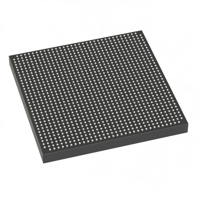
5SGXMA7K2F40C1N
| Part Description |
Stratix® V GX Field Programmable Gate Array (FPGA) IC 696 51200000 622000 1517-BBGA, FCBGA |
|---|---|
| Quantity | 665 Available (as of June 15, 2026) |

| Product Category | Field Programmable Gate Array (FPGA) |
|---|---|
| Manufacturer | Intel |
| Manufacturing Status | Obsolete |
| Manufacturer Standard Lead Time | Contact Us |
| Datasheet |
Specifications & Environmental
| Device Package | 1517-FBGA (40x40) | Grade | Commercial | Operating Temperature | 0°C – 85°C | ||
|---|---|---|---|---|---|---|---|
| Package / Case | 1517-BBGA, FCBGA | Number of I/O | 696 | Voltage | 870 mV - 930 mV | ||
| Mounting Method | Surface Mount | RoHS Compliance | RoHS Compliant | REACH Compliance | REACH Unknown | ||
| Moisture Sensitivity Level | 3 (168 Hours) | Number of LABs/CLBs | 234720 | Number of Logic Elements/Cells | 622000 | ||
| Number of Gates | N/A | ECCN | 3A001A2C | HTS Code | 8542.39.0001 | ||
| Qualification | N/A | Total RAM Bits | 51200000 |
Overview of 5SGXMA7K2F40C1N – Stratix V GX FPGA, 622000 logic elements, 1517-FBGA
The 5SGXMA7K2F40C1N is a Stratix® V GX field-programmable gate array (FPGA) from Intel, offered in a 1517-ball FCBGA package. This commercial-grade device integrates a very high logic capacity with substantial on-chip memory and a large I/O complement for complex, programmable digital designs.
With 622,000 logic elements, approximately 51.2 Mbits of embedded memory, and 696 I/O pins, this FPGA targets high-density applications that require significant local memory, extensive connectivity, and flexible programmable logic resources while operating within a 0 °C to 85 °C temperature range.
Key Features
- Logic Capacity — 622,000 logic elements to implement large, complex logic designs and custom hardware accelerators.
- On-chip Memory — Approximately 51.2 Mbits of embedded RAM for data buffering, packet processing, and local storage of intermediate results.
- I/O Density — 696 user I/O pins to support wide parallel interfaces, multi-channel connectivity, and board-level routing flexibility.
- Package Options — 1517-BBGA (FCBGA) / 1517-FBGA (40×40) supplier device package for high-pin-count board implementations.
- Power and Core Voltage — Core supply range specified from 870 mV to 930 mV to support regulated power delivery for Stratix V GX devices.
- Operating Grade and Temperature — Commercial grade device rated for 0 °C to 85 °C operation.
- Mounting Type — Surface-mount package suitable for modern PCB assembly processes.
- Regulatory Status — RoHS compliant.
Typical Applications
- High-performance networking — Large logic capacity and abundant I/O support packet processing engines, protocol offloads, and wide data buses.
- Data center acceleration — Substantial embedded memory and logic resources can be used to implement hardware accelerators and custom data-paths.
- Telecommunications and communications systems — High I/O count and programmable fabric suit multi-channel interfaces and protocol handling.
- Prototyping and advanced R&D — Commercial-grade Stratix V GX device for evaluating large-scale FPGA architectures and system-level integration.
Unique Advantages
- Extensive programmable resources: 622,000 logic elements provide headroom for complex state machines, DSP chains, and custom compute logic.
- Large embedded memory: Approximately 51.2 Mbits of on-chip RAM reduces external memory dependence and improves data locality for performance-critical tasks.
- High I/O count: 696 I/O pins enable wide parallel interfaces and flexible system partitioning without immediate need for external multiplexing.
- High-density package: 1517-ball FCBGA packaging delivers a compact, high-pin-count solution for space-constrained PCBs.
- Commercial temperature rating: Designed for standard commercial environments with an operating range of 0 °C to 85 °C.
- RoHS compliant: Meets common environmental compliance requirements for modern electronics manufacturing.
Why Choose 5SGXMA7K2F40C1N?
The 5SGXMA7K2F40C1N positions itself as a high-capacity, commercial-grade Stratix V GX FPGA for designers who need substantial logic density, generous embedded memory, and a high I/O count in a compact FCBGA package. Its specified core voltage range and RoHS compliance make it appropriate for production designs that require clearly defined electrical and environmental characteristics.
This device is well suited to teams building large, programmable digital systems—where local memory, parallel connectivity, and programmable logic density are primary design drivers. Backed by Intel’s Stratix V family documentation, it provides a defined platform for scaling FPGA-based solutions in communications, acceleration, and high-density digital applications.
Request a quote or submit an inquiry for pricing and availability for the 5SGXMA7K2F40C1N to move your design forward.


Date Founded: 1968
Headquarters: Santa Clara, California, USA
Employees: 130,000+
Revenue: $54.23 Billion
Certifications and Memberships: ISO9001:2015, ISO14001:2015, ISO17025:2017, ISO27001:2022, ISO45001:2018, ISO50001:2018


