
5SGXMA7K2F35I3N
| Part Description |
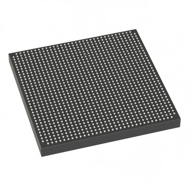
Stratix® V GX Field Programmable Gate Array (FPGA) IC 432 51200000 622000 1152-BBGA, FCBGA |
|---|---|
| Quantity | 1,415 Available (as of June 17, 2026) |
| Product Category | Field Programmable Gate Array (FPGA) |
|---|---|
| Manufacturer | Intel |
| Manufacturing Status | Obsolete |
| Manufacturer Standard Lead Time | Contact Us |
| Datasheet |
Specifications & Environmental
| Device Package | 1152-FBGA (35x35) | Grade | Industrial | Operating Temperature | -40°C – 100°C | ||
|---|---|---|---|---|---|---|---|
| Package / Case | 1152-BBGA, FCBGA | Number of I/O | 432 | Voltage | 820 mV - 880 mV | ||
| Mounting Method | Surface Mount | RoHS Compliance | RoHS Compliant | REACH Compliance | REACH Unknown | ||
| Moisture Sensitivity Level | 3 (168 Hours) | Number of LABs/CLBs | 234720 | Number of Logic Elements/Cells | 622000 | ||
| Number of Gates | N/A | ECCN | 3A001A2C | HTS Code | 8542.39.0001 | ||
| Qualification | N/A | Total RAM Bits | 51200000 |
Overview of 5SGXMA7K2F35I3N – Stratix® V GX FPGA, 622,000 logic elements, 1152‑BBGA FCBGA
The 5SGXMA7K2F35I3N is a Stratix V GX field-programmable gate array (FPGA) in a 1152‑BBGA FCBGA package, rated for industrial operation. It integrates a high logic capacity and substantial on-chip RAM to support complex digital designs requiring large programmable logic and memory resources.
Typical design targets include high-density embedded logic, large buffering and memory-intensive functions, and applications that require a broad set of user I/Os and industrial temperature operation.
Key Features
- Logic Capacity Approximately 622,000 logic elements suited for large-scale custom logic and complex datapath implementations.
- Embedded Memory Approximately 51.2 Mbits of on-chip RAM to support large FIFOs, buffering, and memory-mapped logic functions.
- User I/Os 432 user I/O pins providing extensive external connectivity for peripherals, board-level interfaces, and multi-channel I/O requirements.
- Package & Mounting 1152‑BBGA, FCBGA package (supplier package: 1152‑FBGA (35×35)) with surface-mount mounting for high-density board integration.
- Power Core supply range specified at 820 mV to 880 mV for system power planning and regulator selection.
- Industrial Temperature Grade Rated for operation from −40°C to 100°C to meet elevated ambient and industrial environment requirements.
- Compliance RoHS compliant for regulatory and manufacturing considerations.
Typical Applications
- Networking & Communications Deploys programmable logic and abundant I/O for custom packet processing, protocol bridging, and interface aggregation in communication equipment.
- High‑Performance Embedded Systems Supports compute- and memory-intensive accelerator functions where large logic capacity and on-chip RAM are required.
- Industrial Automation Industrial temperature rating and extensive I/O make it suitable for control systems, motion control, and real-time data aggregation in industrial environments.
- Video & Signal Processing Large logic and memory resources enable implementation of multi-channel video pipelines, image processing, and DSP-centric datapaths.
Unique Advantages
- High Logic Density: 622,000 logic elements enable complex state machines, deep pipelines, and wide datapaths within a single device.
- Substantial Embedded Memory: Approximately 51.2 Mbits of on-chip RAM reduces external memory dependency for buffering and local storage.
- Large I/O Count: 432 user I/Os simplify board routing and reduce the need for external serializers or multiplexers in multi‑interface designs.
- Industrial Robustness: Rated for −40°C to 100°C operation, supporting deployments in demanding temperature environments.
- Compact, High‑Density Package: 1152‑BBGA FCBGA (35×35) enables dense PCB layouts while preserving extensive connectivity.
- Regulatory Compatibility: RoHS compliance supports manufacturing and environmental requirements.
Why Choose 5SGXMA7K2F35I3N?
The 5SGXMA7K2F35I3N combines high programmable logic capacity, significant embedded memory, and a large I/O complement in an industrial‑rated Stratix V GX device package. Its power and thermal characteristics, along with RoHS compliance and surface-mount 1152‑BBGA packaging, make it well suited for engineers designing complex, memory‑intensive systems that must operate reliably across a wide temperature range.
This device is appropriate for development teams and systems integrators targeting high-density FPGA implementations that require scalability, extensive I/O, and on-chip memory to reduce external components and simplify board-level design.
Request a quote or submit an inquiry to get pricing, availability, and support information for 5SGXMA7K2F35I3N.


Date Founded: 1968
Headquarters: Santa Clara, California, USA
Employees: 130,000+
Revenue: $54.23 Billion
Certifications and Memberships: ISO9001:2015, ISO14001:2015, ISO17025:2017, ISO27001:2022, ISO45001:2018, ISO50001:2018


