
5SGXMA7K3F40I3N
| Part Description |
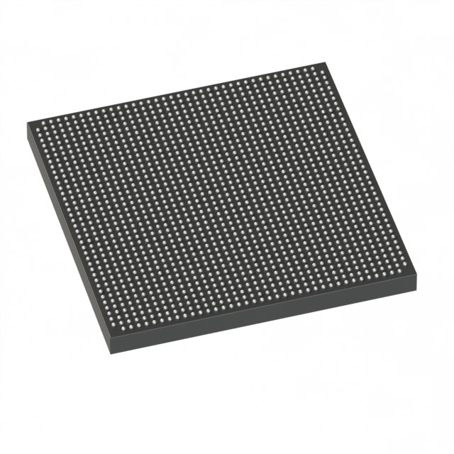
Stratix® V GX Field Programmable Gate Array (FPGA) IC 696 51200000 622000 1517-BBGA, FCBGA |
|---|---|
| Quantity | 826 Available (as of June 15, 2026) |

| Product Category | Field Programmable Gate Array (FPGA) |
|---|---|
| Manufacturer | Intel |
| Manufacturing Status | Obsolete |
| Manufacturer Standard Lead Time | Contact Us |
| Datasheet |
Specifications & Environmental
| Device Package | 1517-FBGA (40x40) | Grade | Industrial | Operating Temperature | -40°C – 100°C | ||
|---|---|---|---|---|---|---|---|
| Package / Case | 1517-BBGA, FCBGA | Number of I/O | 696 | Voltage | 820 mV - 880 mV | ||
| Mounting Method | Surface Mount | RoHS Compliance | RoHS Compliant | REACH Compliance | REACH Unknown | ||
| Moisture Sensitivity Level | 3 (168 Hours) | Number of LABs/CLBs | 234720 | Number of Logic Elements/Cells | 622000 | ||
| Number of Gates | N/A | ECCN | 3A001A2C | HTS Code | 8542.39.0001 | ||
| Qualification | N/A | Total RAM Bits | 51200000 |
Overview of 5SGXMA7K3F40I3N – Stratix V GX FPGA, 622,000 logic elements, ≈51.2 Mbits RAM, 696 I/Os
The 5SGXMA7K3F40I3N is a Stratix® V GX Field Programmable Gate Array (FPGA) IC designed for industrial-grade FPGA applications. It delivers very high logic capacity, large on-chip memory, and extensive I/O resources in a 1517-ball FCBGA package.
Targeted at industrial systems that require high-density programmable logic and broad interfacing, this device combines 622,000 logic elements, approximately 51.2 Mbits of embedded memory, and 696 I/Os to support complex custom hardware functions and dense integration.
Key Features
- Logic Capacity — 622,000 logic elements to implement large-scale digital systems and complex algorithms.
- Logic Array Blocks — 234,720 logic array blocks provide structured building blocks for resource allocation and floorplanning.
- Embedded Memory — Approximately 51.2 Mbits of on-chip RAM to support buffers, FIFOs, and large local storage without external memory.
- I/O Resources — 696 I/Os to accommodate high pin-count interfacing and multi-protocol system integration.
- Package & Mounting — 1517-BBGA (FCBGA) package, supplier device package 1517-FBGA (40×40), surface-mount mounting for compact board-level integration.
- Power — Core voltage supply range: 820 mV to 880 mV, enabling defined core power domain design.
- Industrial Temperature Grade — Rated for operation from −40 °C to 100 °C for deployment in industrial environments.
- RoHS Compliant — Meets current RoHS environmental requirements.
Typical Applications
- Industrial Control & Automation — Industrial temperature rating and large I/O counts make the device suitable for programmable control, motion control, and factory automation interfaces.
- High-Density Signal Processing — Large logic capacity and substantial on-chip RAM support DSP pipelines, packet processing, and real-time data manipulation.
- Communications & Networking Equipment — Extensive I/O resources and high logic density enable protocol handling, packet switching, and custom acceleration in network appliances.
- Custom Hardware Acceleration — Use the device to offload compute-intensive functions with large logic and memory resources for application-specific acceleration.
Unique Advantages
- Significant Logic Density: 622,000 logic elements allow implementation of large, integrated FPGA designs without partitioning across multiple devices.
- Large On-Chip Memory: Approximately 51.2 Mbits of embedded RAM reduces reliance on external memory for high-bandwidth buffering and state storage.
- Extensive I/O Count: 696 I/Os provide flexibility for multi-interface systems and dense connector layouts.
- Industrial Reliability: Industrial temperature rating (−40 °C to 100 °C) supports deployment in harsh and temperature-variable environments.
- Compact BGA Footprint: 1517-ball FCBGA (40×40) package balances high pin-count and compact PCB area for space-constrained designs.
- Defined Core Power Window: 820 mV–880 mV supply range provides clear parameters for power-supply design and thermal planning.
Why Choose 5SGXMA7K3F40I3N?
The 5SGXMA7K3F40I3N positions itself as a high-capacity, industrial-grade Stratix V GX FPGA designed for systems that demand large programmable logic, substantial embedded memory, and a high number of I/Os. Its combination of 622,000 logic elements, approximately 51.2 Mbits of on-chip RAM, and 696 I/Os makes it well suited for complex signal processing, communications, and industrial control applications.
With a surface-mount 1517-ball FCBGA package, a defined core voltage range, and RoHS compliance, this device supports dense hardware integration and application deployments across industrial temperature ranges, offering a scalable foundation for advanced FPGA-based designs.
If you would like pricing or availability for 5SGXMA7K3F40I3N, request a quote or submit a pricing inquiry today.


Date Founded: 1968
Headquarters: Santa Clara, California, USA
Employees: 130,000+
Revenue: $54.23 Billion
Certifications and Memberships: ISO9001:2015, ISO14001:2015, ISO17025:2017, ISO27001:2022, ISO45001:2018, ISO50001:2018


