
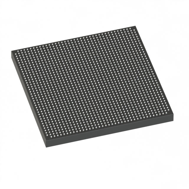
5SGXMA9K2H40C2G
| Part Description |
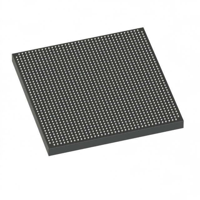
Stratix® V GX Field Programmable Gate Array (FPGA) IC 696 53248000 840000 1517-BBGA, FCBGA |
|---|---|
| Quantity | 562 Available (as of October 8, 2026) |
| Product Category | Field Programmable Gate Array (FPGA) |
|---|---|
| Manufacturer | Intel |
| Manufacturing Status | Active |
| Manufacturer Standard Lead Time | 26 Weeks |
| Datasheet |
Specifications & Environmental
| Device Package | 1517-HBGA (45x45) | Grade | Commercial | Operating Temperature | 0°C – 85°C | ||
|---|---|---|---|---|---|---|---|
| Package / Case | 1517-BBGA, FCBGA | Number of I/O | 696 | Voltage | 870 mV - 930 mV | ||
| Mounting Method | Surface Mount | RoHS Compliance | RoHS Compliant | REACH Compliance | REACH Unaffected | ||
| Moisture Sensitivity Level | 3 (168 Hours) | Number of LABs/CLBs | 317000 | Number of Logic Elements/Cells | 840000 | ||
| Number of Gates | N/A | ECCN | N/A | HTS Code | N/A | ||
| Qualification | N/A | Total RAM Bits | 53248000 |
Overview of 5SGXMA9K2H40C2G – Stratix® V GX Field Programmable Gate Array (FPGA) IC
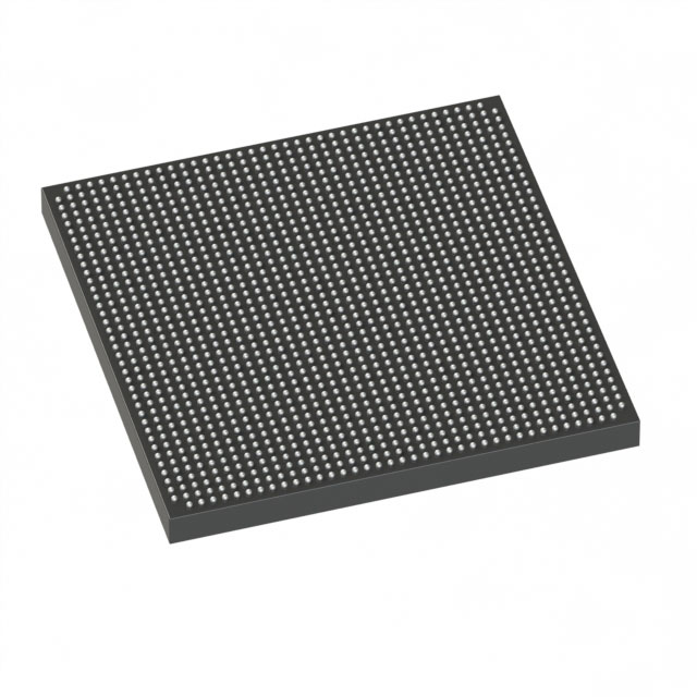
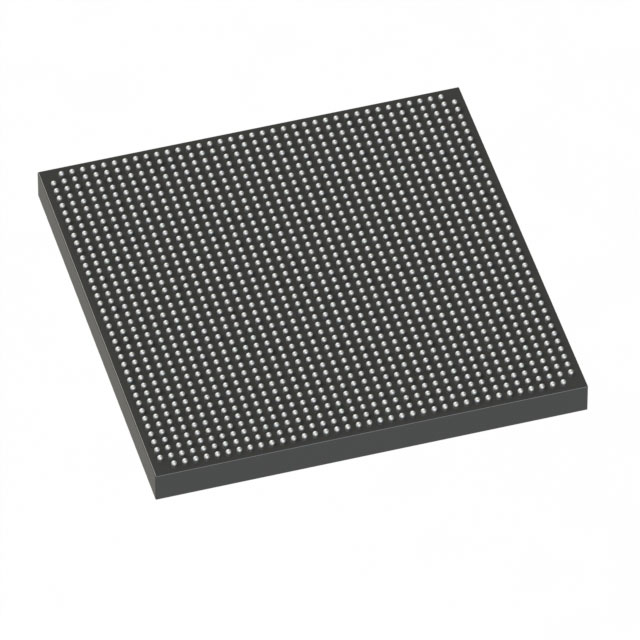
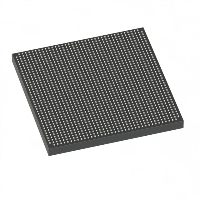
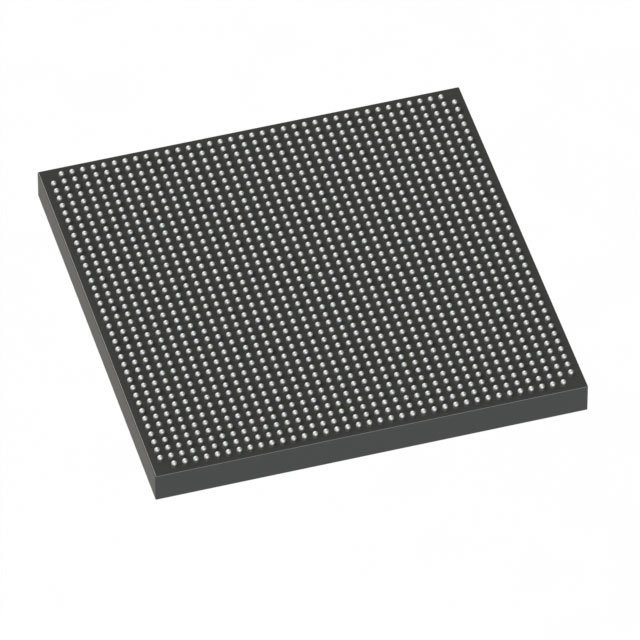
The 5SGXMA9K2H40C2G is a Stratix V GX family FPGA offering high-density programmable logic, substantial on-chip memory, and very large I/O capacity in a 1517-BBGA FCBGA package. This commercial-grade device is engineered for designs that require extensive logic resources, large embedded RAM, and high pin counts in a surface-mount, RoHS-compliant package.
Key value propositions include approximately 840,000 logic elements, roughly 53.25 Mbits of embedded memory, and 696 I/O pins, combined with a low-voltage core supply range (870 mV–930 mV) and a commercial operating temperature window (0 °C–85 °C) for predictable board-level integration.
Key Features
- Core Capacity Approximately 840,000 logic elements and 317,000 logic array blocks (LABs) provide high-density programmable logic for complex designs.
- Embedded Memory Approximately 53.25 Mbits of on-chip RAM to support large buffering, state storage, and data-path implementations without excessive external memory.
- I/O Resources 696 user I/O pins for broad connectivity and high channel count designs.
- Power Core voltage supply range of 870 mV to 930 mV to support the device’s power requirements.
- Package & Mounting 1517-BBGA FCBGA package, supplier device package 1517-HBGA (45×45), surface-mount for compact board integration.
- Operating Grade & Temperature Commercial grade with an operating temperature range of 0 °C to 85 °C.
- Regulatory RoHS compliant.
Typical Applications
- High‑performance signal processing Use large logic and embedded RAM capacity to implement DSP pipelines, custom accelerators, and complex data-path logic.
- Network and communications platforms High I/O count and Stratix V GX family characteristics support dense interfacing and multi-channel data routing.
- Compute acceleration and offload Leverage extensive logic resources and on-chip memory to implement application-specific acceleration functions on system boards.
- Test and measurement equipment Combine high logic density and wide I/O to create flexible, programmable instrumentation and data acquisition solutions.
Unique Advantages
- High-density programmable fabric: Approximately 840,000 logic elements enable complex, large-scale designs without fragmenting logic across multiple devices.
- Substantial embedded RAM: Roughly 53.25 Mbits of on-chip memory reduces reliance on external RAM for buffering and stateful operations.
- Extensive I/O capability: 696 I/Os provide design flexibility for multi-channel interfaces and high-pin-count systems.
- Compact, production-ready package: 1517-BBGA (45×45) surface-mount package simplifies board-level assembly while supporting high integration density.
- Commercial temperature and RoHS compliance: Clearly defined operating range (0 °C–85 °C) and environmental compliance support mainstream product deployments.
- Predictable power domain: Specified core voltage range (870 mV–930 mV) helps with power supply planning and thermal budgeting.
Why Choose 5SGXMA9K2H40C2G?
This Stratix V GX FPGA part combines very large logic resources, significant embedded memory, and a high I/O count in a single commercial-grade FCBGA package, making it suitable for demanding board-level designs that require dense programmable logic and extensive interfacing. The device’s defined electrical and thermal parameters support predictable integration into systems with tight resource and layout constraints.
Designers targeting high-channel, high-throughput, or memory-intensive FPGA implementations will find the 5SGXMA9K2H40C2G appropriate for scalable, long-term deployments that benefit from the Stratix V ecosystem and documented device characteristics.
Request a quote or submit an inquiry to get pricing and availability information for the 5SGXMA9K2H40C2G and to evaluate its fit for your next design.





















Date Founded: 1968
Headquarters: Santa Clara, California, USA
Employees: 130,000+
Revenue: $54.23 Billion
Certifications and Memberships: ISO9001:2015, ISO14001:2015, ISO17025:2017, ISO27001:2022, ISO45001:2018, ISO50001:2018


