
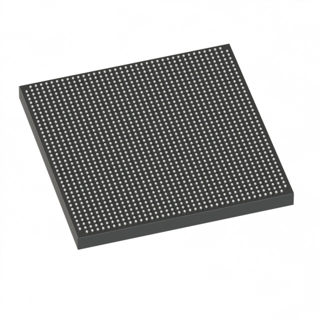
5SGXMB5R2F40C2LN
| Part Description |
Stratix® V GX Field Programmable Gate Array (FPGA) IC 432 41984000 490000 1517-FBGA (40x40) |
|---|---|
| Quantity | 1,113 Available (as of June 18, 2026) |

| Product Category | Field Programmable Gate Array (FPGA) |
|---|---|
| Manufacturer | Intel |
| Manufacturing Status | Obsolete |
| Manufacturer Standard Lead Time | Contact Us |
| Datasheet |
Specifications & Environmental
| Device Package | 1517-FBGA (40x40) | Grade | Commercial | Operating Temperature | 0°C – 85°C | ||
|---|---|---|---|---|---|---|---|
| Package / Case | 1517-FBGA (40x40) | Number of I/O | 432 | Voltage | 820 mV - 880 mV | ||
| Mounting Method | Surface Mount | RoHS Compliance | RoHS Compliant | REACH Compliance | REACH Unknown | ||
| Moisture Sensitivity Level | 3 (168 Hours) | Number of LABs/CLBs | 185000 | Number of Logic Elements/Cells | 490000 | ||
| Number of Gates | N/A | ECCN | 3A001A2C | HTS Code | 8542.39.0001 | ||
| Qualification | N/A | Total RAM Bits | 41984000 |
Overview of 5SGXMB5R2F40C2LN – Stratix® V GX Field Programmable Gate Array (FPGA) IC, 1517-FBGA (40×40)
The 5SGXMB5R2F40C2LN is a Stratix V GX family FPGA in a 1517-FBGA (40×40) surface-mount package. It delivers a very large programmable logic array—490,000 logic elements—and substantial embedded memory for complex, memory‑intensive designs.
Designed for commercial-temperature applications, the device provides a high I/O count (432 pins), low core-voltage operation (820 mV to 880 mV), and the Stratix V GX series transceiver options described in the device datasheet for multi‑gigabit serial interfaces.
Key Features
- Core Logic Capacity Approximately 490,000 logic elements to implement large, highly parallel logic designs.
- Embedded Memory Approximately 42 Mbits of on-chip RAM for buffering, packet processing, and intermediate data storage within logic designs.
- I/O Density 432 user I/O pins enable wide external interface connectivity and complex multi‑lane I/O topologies.
- Transceiver Capability (Series) Stratix V GX devices are documented with multi‑Gbps transceiver speed grades in the datasheet, supporting high‑speed serial links for communications and networking applications.
- Low-Voltage Core Core supply range of 820 mV to 880 mV for compatibility with low-voltage system designs and efficient core power delivery.
- Package & Mounting 1517‑FBGA (40×40) package in a surface-mount form factor to support compact, board-level integration.
- Commercial Temperature Grade Rated for 0 °C to 85 °C operation, suitable for standard commercial environments.
- RoHS Compliant Meets RoHS requirements for lead‑free manufacturing processes.
Typical Applications
- High‑speed communications Multi‑gigabit serial transceiver options in the Stratix V GX series make this device suitable for line cards, switches, and high‑bandwidth I/O aggregation where many lanes and high throughput are required.
- Compute acceleration and DSP Large logic capacity and tens of Mbits of on‑chip RAM support dense DSP pipelines, hardware accelerators, and packet processing engines.
- Prototyping and custom logic Reconfigurable FPGA fabric enables rapid hardware prototyping and deployment of custom algorithms without ASIC turnaround.
- Complex I/O and protocol bridging High I/O pin count supports diverse interface standards and multi‑channel bridging or aggregation tasks on a single device.
Unique Advantages
- High integration density: Consolidate large amounts of logic and memory into a single 1517‑FBGA device, reducing board component count and design complexity.
- Large on‑chip memory: Approximately 42 Mbits of embedded RAM reduces external memory bandwidth needs and lowers system latency for buffer‑intensive functions.
- Extensive I/O capability: 432 I/Os provide flexibility to connect multiple peripherals, SerDes lanes, or parallel interfaces without external multiplexing.
- Low core-voltage operation: 820 mV–880 mV core supply supports power-optimized designs and aligns with modern low‑voltage power distribution strategies.
- Commercial-grade reliability: Rated for 0 °C to 85 °C operation and RoHS compliant for standard commercial product deployments.
Why Choose 5SGXMB5R2F40C2LN?
The 5SGXMB5R2F40C2LN positions itself as a high‑capacity, memory‑rich Stratix V GX FPGA for commercial applications that demand large programmable logic resources, substantial on‑chip memory, and broad I/O capability. Its low core‑voltage operation and FBGA package support compact, power-conscious designs.
This device is well suited to customers developing high‑throughput communications equipment, hardware accelerators, and complex system prototypes that benefit from the Scalability and configurability of Stratix V GX family devices. The datasheet for the Stratix V family provides detailed electrical and transceiver specifications to support system-level design and integration choices.
Request a quote or submit a price inquiry to begin evaluating the 5SGXMB5R2F40C2LN for your next design project.


Date Founded: 1968
Headquarters: Santa Clara, California, USA
Employees: 130,000+
Revenue: $54.23 Billion
Certifications and Memberships: ISO9001:2015, ISO14001:2015, ISO17025:2017, ISO27001:2022, ISO45001:2018, ISO50001:2018


