
5SGXMB6R1F40C1G
| Part Description |
Stratix® V GX Field Programmable Gate Array (FPGA) IC 432 53248000 597000 1517-FBGA (40x40) |
|---|---|
| Quantity | 87 Available (as of June 15, 2026) |

| Product Category | Field Programmable Gate Array (FPGA) |
|---|---|
| Manufacturer | Intel |
| Manufacturing Status | Active |
| Manufacturer Standard Lead Time | 26 Weeks |
| Datasheet |
Specifications & Environmental
| Device Package | 1517-FBGA (40x40) | Grade | Commercial | Operating Temperature | 0°C – 85°C | ||
|---|---|---|---|---|---|---|---|
| Package / Case | 1517-FBGA (40x40) | Number of I/O | 432 | Voltage | 870 mV - 930 mV | ||
| Mounting Method | Surface Mount | RoHS Compliance | RoHS Compliant | REACH Compliance | REACH Unaffected | ||
| Moisture Sensitivity Level | 3 (168 Hours) | Number of LABs/CLBs | 225400 | Number of Logic Elements/Cells | 597000 | ||
| Number of Gates | N/A | ECCN | N/A | HTS Code | N/A | ||
| Qualification | N/A | Total RAM Bits | 53248000 |
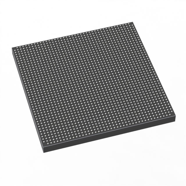
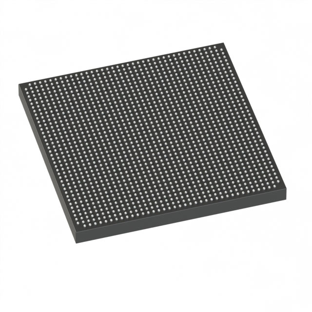
Overview of 5SGXMB6R1F40C1G – Stratix V GX FPGA, 597,000 logic elements, 1517-FBGA
The 5SGXMB6R1F40C1G is a Stratix® V GX Field Programmable Gate Array (FPGA) IC from Intel. It delivers a large programmable logic resource set and substantial on-chip memory in a compact 1517-FBGA (40x40) surface-mount package.
With 597,000 logic elements, approximately 53 Mbits of embedded RAM, and 432 I/O pins, this commercial-grade FPGA is suited for designs that require high integration density, significant embedded memory, and extensive I/O connectivity while operating within a commercial temperature range.
Key Features
- Logic Capacity Approximately 597,000 logic elements for complex, high-density logic implementations.
- Embedded Memory Approximately 53 Mbits of on-chip RAM (53,248,000 bits) to support data buffering, large state machines, and memory-intensive functions.
- I/O Resources 432 I/O pins to support broad peripheral and interface connectivity.
- Power / Core Voltage Core supply range: 870 mV to 930 mV, enabling precise power management and system integration.
- Package & Mounting 1517-FBGA (40x40) package in a surface-mount form factor for compact board-level integration.
- Temperature & Grade Commercial grade device with an operating temperature range of 0°C to 85°C.
- Regulatory Compliance RoHS compliant.
Unique Advantages
- High logic density: Large pool of logic elements supports complex FPGA implementations without external logic proliferation.
- Substantial embedded memory: Approximately 53 Mbits of on-chip RAM reduces dependence on external memory for many applications.
- Extensive I/O count: 432 I/Os provide flexibility for interfacing with multiple peripherals, sensors, or high-pin-count subsystems.
- Compact, solderable package: The 1517-FBGA (40x40) surface-mount package enables dense PCB layouts and streamlined mechanical integration.
- Commercial temperature suitability: Rated for 0°C to 85°C, aligning with a wide range of commercial electronics environments.
- Environmental compliance: RoHS compliance supports regulatory and sustainability requirements.
Why Choose 5SGXMB6R1F40C1G?
The 5SGXMB6R1F40C1G positions itself as a highly integrated Stratix V GX FPGA option for designs that need a large logic fabric, significant on-chip memory, and extensive I/O in a compact FBGA package. Its core voltage range, commercial temperature rating, and RoHS compliance make it appropriate for many commercial electronics applications where density and integration are priorities.
Backed by Intel's Stratix V device documentation, this device is suitable for teams seeking a documented, high-capacity FPGA silicon option that can scale within the Stratix V family framework and integrate into dense PCB designs.
Request a quote or submit an inquiry to obtain pricing, availability, and integration details for the 5SGXMB6R1F40C1G.


Date Founded: 1968
Headquarters: Santa Clara, California, USA
Employees: 130,000+
Revenue: $54.23 Billion
Certifications and Memberships: ISO9001:2015, ISO14001:2015, ISO17025:2017, ISO27001:2022, ISO45001:2018, ISO50001:2018


